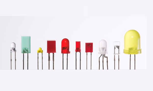
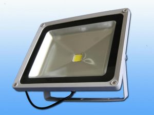
 Definition of COB
COB is the chip on board, which is to attach the bare chip to the interconnect substrate with conductive or non-conductive glue, and then wire bonding to achieve its electrical connection. There are three package types: long, square, and round.
COB production process
The COB LED surface light source firstly covers the silicon wafer placement point with a thermally conductive epoxy (generally an epoxy resin doped with silver particles) on the surface of the substrate, and then directly places the silicon wafer on the surface of the substrate, and heat-treats the silicon wafer to be firmly fixed on the substrate. So far, a wire bonding method is used to directly establish an electrical connection between the silicon wafer and the substrate. There are two main forms of bare chip technology: one is COB technology, and the other is Flip Chip technology. Chip-on-board packaging (COB), where semiconductor chips are handed over and mounted on a printed circuit board. The electrical connection between the chip and the substrate is realized by a wire stitching method. The electrical connection between the chip and the substrate is realized by a wire stitching method, and covered with resin to ensure reliability. . Although COB is the simplest bare chip placement technology, it has a packaging density that is far inferior to TAB and flip-chip bonding technologies.
Definition of MCOB
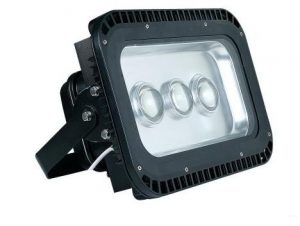 MCOB (Muilti Chips On Board), which is a multi-cup integrated COB packaging technology, is an extension of the COB packaging process. MCOB packaging puts the chip directly in the optical cup, and coats each single chip with phosphor and Finish dispensing and other processes. The LED chip light is concentrated inside the cup. To allow more light to run out, the more light exits, the higher the light efficiency. The efficiency of MCOB low-power chip packages is generally higher than that of high-power chips Packaging efficiency. It directly places the chip on a heat sink such as a metal substrate, thereby shortening the heat dissipation path, reducing thermal resistance, improving the heat dissipation effect, and effectively reducing the junction temperature of the light emitting chip.
Definition of SMD LED
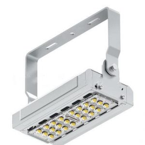 SMD LED is the meaning of surface-mount light-emitting diodes. SMD patches help improve production efficiency and applications in different facilities. It is a solid-state semiconductor device that can directly convert electricity into light. Its voltage is 1.9-3.2V, and the red and yellow voltages are the lowest. The heart of the LED is a semiconductor wafer. One end of the wafer is attached to a bracket, one end is the negative electrode, and the other end is connected to the positive electrode of the power supply. Encapsulated in epoxy resin. A semiconductor wafer is composed of two parts, one is a P-type semiconductor, in which holes dominate, and the other is an N-type semiconductor, which is mainly electrons. But when these two semiconductors are connected, a P-N junction is formed between them. When a current is applied to the wafer through a wire, electrons are pushed to the P region, where the electrons and holes recombine, and then energy is emitted in the form of photons. This is the principle of LED light emission. The wavelength of light, which is the color of light, is determined by the material that forms the P-N junction.
Difference and comparison of SMD,COB and MCOB in LED
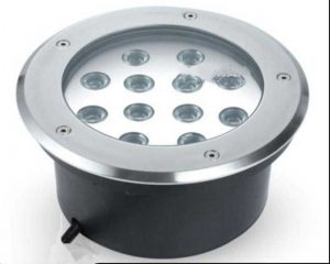 LEDs have entered the lighting field since the initial form was that the beads were directly welded to the board, first 3528, 5050, and then 3014, 2835. However, the disadvantages of this method are that there are many processes, LED packaging and SMT, high cost, and heat transfer problems. Therefore, COB was introduced into the LED field at this time. | Traditional LED: “LED discrete components → MCPCB light source module → LED lamps”, mainly due to the lack of ready-made suitable core light source components, the approach is not only time-consuming and costly. COB package “COB light source module → LED lamp”, which can directly package multiple chips on the metal-based printed circuit board MCPCB, and directly dissipate heat through the substrate, saving the cost of primary packaging of the LED, the manufacturing cost of the light bow and the module Light cost. In terms of performance, through reasonable design and micro-lens molding, the COB light source module can effectively avoid the disadvantages of point light and glare in the combination of discrete light source devices; it can also add appropriate red chip combinations without significantly reducing the efficiency of the light source and Under the premise of life, effectively improve the color rendering of the light source.
In the LED lighting industry, SMD (Surface Mounted Devices), LED SMD means surface-mount light-emitting diodes, with a large light emitting angle, which can reach 120-160 degrees. Compared with earlier plug-in packages, it has high efficiency, good precision, and false soldering Low rate, light weight, small size, etc.
Difference between LED MCOB package and LED COB package
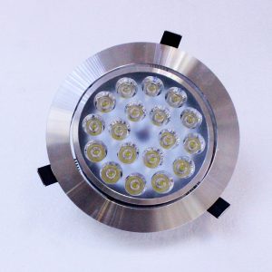 1.The COB package of LED is based on the packaging of the back substrate. It is the integration of N chips on the back substrate for packaging. This is the COB technology that everyone says. You know that the copper substrate is under the back substrate Copper foil can only be energized very well, and can’t do good optical treatment. In terms of light efficiency and cost: COB encapsulates the LED chip into the entire inner substrate. Because the coating of the encapsulant and the phosphor is distributed in a planar shape, it is difficult to excite the phosphors on the edge, and the phosphors are invisible to the phosphor. Use caused a lot of waste.
2.MCOB technology encapsulates the LED chip into an optical cup, learned the essence of LED SMD device dispensing, coated phosphors on each single chip and completed the dispensing process. Using this method, the amount of phosphor used will be Greatly reduced. 1 At the same time, the LED chip light is concentrated inside the chip. The MCOB plane light source is a multi-cup integrated chip, which provides more light outlets and allows light to be emitted from multiple angles. The chip welded on the MCOB aluminum substrate has no insulation layer, and heat is directly introduced into the aluminum layer, and the thermal conductivity of the aluminum layer is 271 ~ 320 w / m.k. The chip of the COB aluminum substrate has the thermal resistance of the insulating layer, and the thermal conductivity of the insulating layer is 0.4 ~ 3.0 w / m.k, which prevents the chip’s heat from being transmitted “down. The heat dissipation is much slower than the MCOB planar light source.
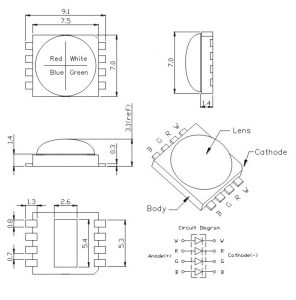 MCOB packaging products: MCOB packaging technology is used. Compared with the traditional COB packaging method, MCOB improves the reflectivity of the holder cup and improves the light output efficiency. Therefore, our products have a particularly high light output efficiency. Under the premise that RA is greater than 80 and color temperature is 2600K, each watt can reach more than 90LM. From the copper lead frame to the ceramic package, a vertically integrated structure is used. The chip is directly fixed on the copper surface, and then the copper on the backside is in direct contact with the heat sink. In this way, the heat dissipation speed is accelerated, and the heat generated on the chip can be better conducted.
What are the advantages of COB comparison:
1.Production efficiency advantage
The production process of COB packaging is basically the same as the traditional SMD production process, and the efficiency of SMD packaging is basically the same in die bonding and wire bonding processes. Products are much higher. Traditional SMD packaging labor and manufacturing costs account for about 15% of material costs, and COB packaging labor and manufacturing costs account for about 10% of material costs. With COB packaging, labor and manufacturing costs can be saved by 5%.
2.Advantages of low thermal resistance
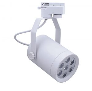 The system thermal resistance of traditional SMD packaging applications is: chip_Zhou Jingjiao-solder joint-solder paste copper foil insulation layer aluminum. The thermal resistance of the COB package system is: chip_solid crystal aluminum. The thermal resistance of the COB package system is much lower than that of the traditional SMD package, which greatly improves the life of the LED.
3.light quality advantages
The traditional SMD package uses a patch to form multiple discrete devices on a PCB to form a light source assembly for LED applications. This method has the problems of point light, glare and ghosting. The COB package is an integrated package and is a surface light source. The viewing angle is large and easy to adjust, which reduces the loss of light refraction. It is also possible to effectively improve the color rendering of the light source by adding an appropriate combination of red chips without significantly reducing the efficiency and life of the light source.
4.Application and cost advantages
Taking a fluorescent tube as an example, it can be seen from the above figure that the COB light source eliminates the process of patch and reflow soldering at the application side, greatly
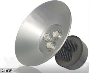 The application-side production and manufacturing process is reduced, and corresponding equipment can be omitted. The manufacturing equipment investment cost is lower and the production efficiency is higher.
Summary At present, there are still many technical problems in COB dispensing, such as heat dissipation, chip-resistance, and phosphor ratio. For areas such as indoor lighting that only require low-power packaged devices, it is still applicable, but when high-power packaged devices are required, such as the lighting of tunnel lights, COB dispensing still cannot replace the existing packaging form.
COB light source and MCOB technology will become mainstream
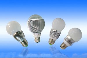 At present, the cost of LED packaging is relatively high, and the overall cost of LED devices is reduced. In addition to materials, a low-cost and efficient packaging structure needs to be selected. The production cost of COB light sources is relatively low, the heat dissipation function is obvious, and it has the characteristics of high packaging density and high optical density. Whether it can become the mainstream of packaging has been the focus of the industry. Compared with traditional LED packaging technology, COB panel light source has very soft light and has a very large market, which is a future development direction. According to surveys, the number of companies doing COB packaging in the market is gradually increasing, and some companies have reached the volume Production. Since last year, the COB light source technology of Japanese manufacturers has greatly improved. Many companies have begun to switch to the COB packaging mode. 00B substrate materials have also been improved. Early copper substrates have been developed to aluminum substrates. The ceramic substrate gradually improves the reliability of the COB light source. In March of this year, Japan’s Citizen launched a multi-chip product, using COB technology, to house multiple blue LED chips in a package, achieving high heat dissipation performance, bringing COB technology to the market again. In addition, Sharp ’s ceramic plate COB, another Japanese manufacturer, has also achieved mass production. It is one of the few energy-producing ceramic COB light sources in Asia. In contrast, although the COB light source has experienced the pains of the last round of development, many companies continue to research and develop and have achieved certain technical results. Li Guoping, chairman of Hongli Optoelectronics, a listed packaging company, said that Hongli Optoelectronics has used a variety of materials such as ceramic substrates and aluminum substrates to develop COB light sources, and has already achieved mass production. The light efficiency has also been greatly improved, and the product reliability is good. “Ceramic substrate can solve the reliability problem of COB very well, but its material cost is relatively high, and it has a certain technical difficulty.”
 Summary:
At present, COB-packaged bulbs have occupied about 40% of the market for LED bulbs. Many Japanese and domestic companies have begun to adopt the COB packaging model, which is an inevitable trend in the future. “He Wenming, Chairman of Fujian Wanbang Optoelectronics Technology Co., Ltd. Emphasized. In addition, COB light sources are not only improved in materials and reliability, and their optical technology has been further improved. Although COB light sources have better heat dissipation functions, the copper foil under the substrate can only be well energized. But it can’t do good optical processing, so some companies have proposed MCOB technology. MCOB light output efficiency is higher than COB light source, and it is expected to become the mainstream of the market. MCOB technology, that is, multi-cup integrated COB packaging technology, is LED cluster packaging technology. The abbreviation of Chips On Board, COB technology is to integrate N chips on a substrate for packaging. However, there is a copper box under the substrate, which cannot perform optical processing well. MCOB directly puts the chips in multiple optical cups. Encapsulation, to improve the luminous flux, can also facilitate the packaging of LED surface light, increase the power of a single light source, the most Limit glare and zebra pattern, and improve the light efficiency per watt. From the current point of view, LED still cannot perfectly solve the core problem of photoelectric conversion efficiency. In addition to adding heat sink components, packaging is the core link to solve the heat dissipation problem. Light source based on COB technology Will become the mainstream of LED lights, is the future technological development direction.

