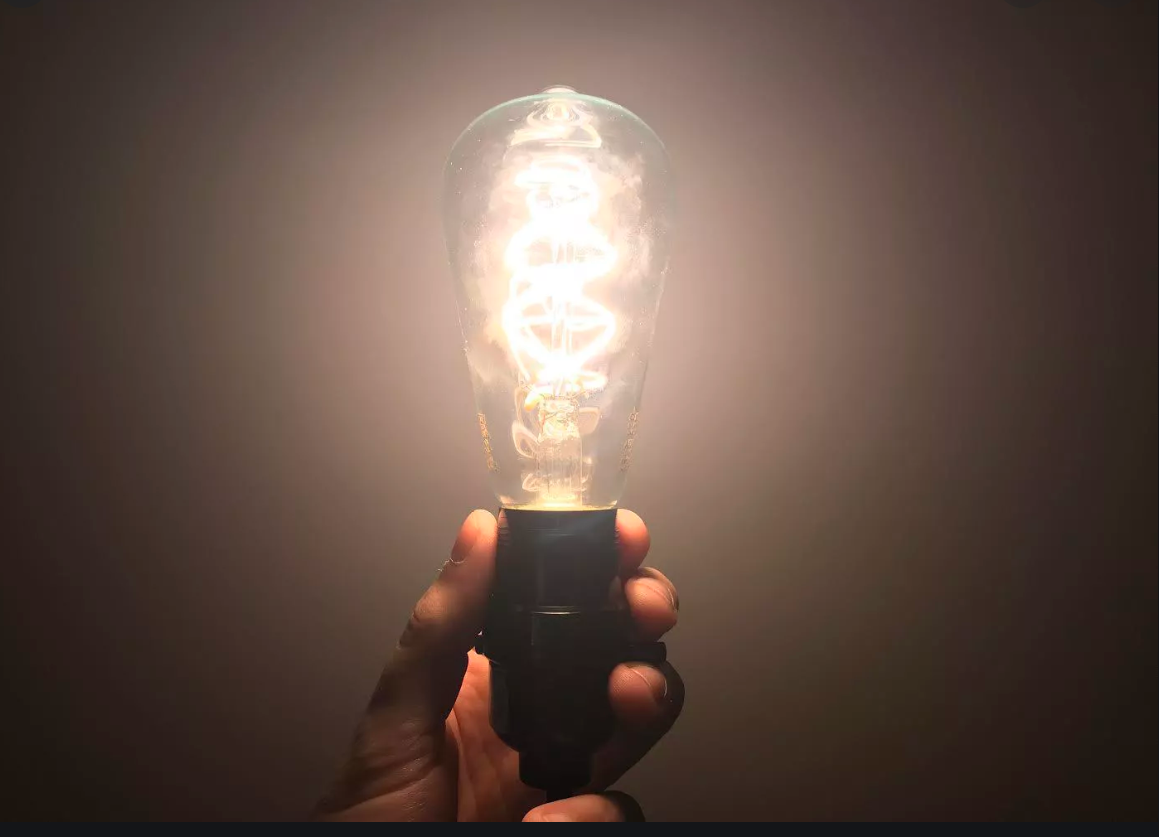
1Lux (lux) refers to the illuminance where 1L of luminous flux is evenly distributed on an area of 1 square meter. Generally, active illuminators use luminous intensity unit candle CD, such as incandescent lamps, LEDs, etc.; reflective or transmissive objects use luminous flux unit lumens L, such as LCD projectors, etc.; and illuminance unit Lux, generally used in photography and other fields .
The three measurement units are equivalent in value, but need to be understood from different angles. For example: if the brightness (luminous flux) of an LCD projector is 1600 lumens, and the size of the projection onto the total reflection screen is 60 inches (1 square meter), its illuminance is 1600 lux, assuming that its light exit is away from the light source 1 cm, the area of the light exit is 1 cm2, the luminous intensity of the light exit is 1600CD. However, the brightness of real LCD projectors will be greatly reduced due to the loss of light propagation, the loss of reflection or light-transmitting film and the uneven light distribution. Generally, an efficiency of 50% is good.
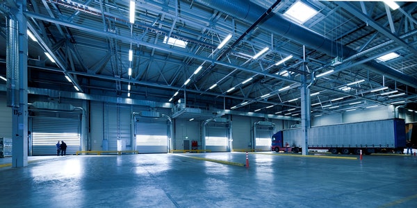
In actual use, light intensity calculations often use data units that are easier to map or change directions. For the active luminous body of the LED screen, CD/meter square is generally used as the luminous intensity unit, and the observation angle is used as the auxiliary parameter, which is equivalent to the lux unit on the surface of the screen; this value is effectively displayed with the screen. Multiply the area to obtain the luminous intensity of the entire screen at the best viewing angle. Assuming that the luminous intensity of each pixel in the screen is constant in the corresponding space, this value can be considered as the luminous flux of the entire screen. Generally, the outdoor LED screen must reach a brightness of 4000CD/m² or more to have an ideal display effect in sunlight. Ordinary indoor LED, the maximum brightness is about 700 ~ 2000 CD/m².
The luminous intensity of a single LED takes CD as the unit and is equipped with viewing angle parameters. The luminous intensity has nothing to do with the color of the LED. The luminous intensity of a single tube varies from a few mCD to 5000 mCD. The luminous intensity given by the LED manufacturer refers to the point where the luminous intensity is the highest at the best viewing angle and at the center position when the LED is lit at a current of 20 mA.
When the LED is packaged, the shape of the top lens and the position of the LED chip from the top lens determine the viewing angle and light intensity distribution of the LED. Generally speaking, the larger the viewing angle of the same LED, the smaller the maximum luminous intensity, but the accumulated luminous flux on the entire three-dimensional hemisphere remains unchanged. When multiple LEDs are arranged closely and regularly, their light-emitting spherical surfaces are superimposed on each other, resulting in a more uniform light-emitting intensity distribution across the entire light-emitting plane.
When calculating the luminous intensity of the screen, it is necessary to multiply the maximum point luminous intensity value provided by the manufacturer by 30% to 90% according to the viewing angle of the LED and the emission density of the LED, as the average luminous intensity of a single tube. Generally, the luminous life of LEDs is very long. Manufacturers generally indicate that it is more than 100,000 hours. In fact, you should also pay attention to the brightness decay cycle of LEDs. For example, most of the UR red tubes used in automobile taillights are lit for more than ten to tens of hours. , The brightness is only half of the original.
The brightness decay cycle has a great relationship with the material process of LED production. Generally, four-element LEDs with slower brightness decay should be selected when economic conditions permit. Color matching and white balance: white is a mixture of red, green and blue according to the brightness ratio. When the brightness of green is 69%, the brightness of red is 21%, and the brightness of blue is 10%, the human eye will feel the color after mixing The result is pure white.
However, the chromaticity coordinates of the red, green, and blue LEDs cannot achieve the full color spectrum effect due to the manufacturing process and other reasons, and controlling the brightness of the primary colors including the deviated primary colors to obtain white light is called color matching. Before color matching for a full-color LED screen, in order to achieve the best brightness and the lowest cost, you should try to choose the LED device composition pixels whose luminous intensity of the three primary colors is roughly 3:6:1.
White balance requires the three primary colors to be synthesized under the same gray value to still be pure white. Primary colors, primary colors: Primary colors refer to the basic colors that can be synthesized into various colors. The primary colors in the color light are red, green, and blue. The figure below is the spectrum table. The three vertices in the table are the ideal primary color wavelengths. If the primary colors are deviated, the area where colors can be synthesized will decrease, and the triangles in the spectrum table will shrink. From a visual point of view, the colors will not only deviate, but also the richness will decrease.
The red, green, and blue rays emitted by LEDs are roughly divided into purple, pure red, orange-red, orange, orange-yellow, yellow, yellow-green, pure green, emerald green, blue-green, pure blue, blue-violet, etc. according to their different wavelength characteristics. , Yellow-green and blue-violet are much cheaper than pure red, pure green and pure blue. Of the three primary colors, green is the most important, because green occupies 69% of the brightness of white and is in the center of the horizontal color list. Therefore, in the three-primary color composition method that weighs the purity of the color and the price, in the three-primary color design application, the white balance and the maximum expected brightness value are usually achieved by adjusting the LED current.
We generally take the simplest and most optimized color matching method as the color reproduction method for designing full-color display technology. White balance is one of the important signs for checking color composition. The three primary colors of white light are generally made by mixing the three primary colors of red, green and blue according to the brightness ratio. When the brightness of green in the light is 69%, the brightness of red is 21%, and the brightness of blue is 10%, the human eye will feel the color after mixing. It is pure white. The early CRT TV sets to the current LCD liquid crystal display are all composed in this way.
Analysis of the influence of CAN semiconductor materials on LED performance
Gan-based semiconductor materials have been widely used in the manufacture of short-wavelength optoelectronic devices in recent years, such as light-emitting diodes (LEDs) and laser diodes (LDs). At present, there are many reports and literatures on the growth of Gan materials, and a few reports on chip manufacturing are only limited to Gan etching and ohmic contacts, and there are few technical reports on engineering design. This paper discusses the impact of chip layout design on the performance of Gan-based LEDs, which can provide a reference for choosing chip layouts for different performance requirements.
experiment
The material we use is a blue Gan-based LED epitaxial wafer grown on a sapphire substrate by the MOCVD method. The epitaxial wafer is a multi-quantum well structure. In chip manufacturing, the n-ohm contact electrode adopts the Ti/Al/Ti/Au structure, the p-ohm contact electrode uses an oxide Ni/Au transparent electrode, and the wire electrode is Ti/Au with a very consistent epitaxial wafer. The mosaic structure layout of 400μm×500μm, the mosaic structure layout of 350μm×350μm and two kinds of 350μm×350μm diagonal layouts were respectively made. The chip characteristic test sample takes the center of the wafer and the quarter of the chip at the apex of the right angle after slicing. The test instrument is a T620 tester produced by Taiwan Changyu Company.
Results and discussion
We tested the I-V characteristics and P-I characteristics of the chips with four layouts, including the I-V characteristic curves and P-I characteristic curves of various layout chips.
It can be seen from the I-V characteristics that below 20mA, the I-V characteristics of the two-size mosaic structure layout chip and the diagonal electrode chip with the p wire electrode in the middle of the extended electrode are basically the same, and the p wire electrode is far away from the n electrode diagonally. The forward voltage drop Vf of the electrode chip under the same current is higher than that of other chips. Although (a) the area of the extended electrode is large, it is beneficial to reduce the p-type ohmic contact resistance, but it increases the distance of current transport, which may increase the body resistance. The two effects offset make the I-V characteristic and size of the chip smaller The layout chip is similar. (A) Using diagonal electrodes, the measured I-V characteristics show that when the distance between the p wire electrode and the n electrode is almost the same, the chip I-V characteristics are equivalent to the mosaic structure electrode chip. (B) The relative Vf of the p wire electrode is far from the n electrode and the diagonal electrode chip is higher, which means that the current density under the p wire electrode is higher than the current density under the extended electrode equidistant from the n electrode. The distance between the n electrodes makes the chip equivalent body resistance larger and Vf higher.
The P-I characteristics of various layout chips show that below 20mA, the P-I characteristics of various Gan-based LED chips are linear, and the P-I characteristics of the two-size mosaic structure layout chip and the diagonal electrode chip are within 30mA. The characteristics of I are basically the same. When the current becomes larger, the optical power of a large-sized chip is greater than that of a small-sized chip. (B) When the p wire electrode is far away from the diagonal electrode chip of the n electrode, the optical power is higher under normal working current (<30mA), but the power saturation is faster under high current.
The PI characteristics of Gan-based LEDs below 20mA are linear. The optical power has nothing to do with the current density, but only depends on the effective current. Although the chip area is different, the current is the same, the luminous efficiency is the same, the optical power is similar, and the size is large. Because the current density of the chip is small under the same current, it has certain advantages to work under high current.
(B) The optical power of the diagonal electrode chip of the layout is higher under the normal working current, indicating that the current density under the extended electrode area near the n electrode is larger, and the p wire electrode is moved away from the n electrode area to increase the light transmittance Part of the current reduces the current in the light-absorbing area under the p wire electrode. Under the condition of high current, on the one hand, the current density is high and it is easy to saturate. On the other hand, due to the large equivalent body resistance, the high current generates heat relatively quickly and the luminous power is more likely to saturate.
Conclusion
Studies have shown that the I-V and PI characteristics of Gan-based LED chips below 20mA have little relationship with the size, but are related to the position of the electrode. The light output power of the chip with the p wire electrode far away from the n electrode is high under 20mA. , The forward pressure drop is also high. Under high current, the chip with the p wire electrode far away from the n electrode is easy to saturate, and the high current performance of the chip with a larger chip size is better. Comparison of the characteristics of the mosaic structure electrode and the diagonal structure electrode chip showed no significant difference.
We use cookies on our website to give you the most relevant experience by remembering your preferences and repeat visits. By clicking “Accept All”, you consent to the use of ALL the cookies. However, you may visit "Cookie Settings" to provide a controlled consent.
This website uses cookies to improve your experience while you navigate through the website. Out of these, the cookies that are categorized as necessary are stored on your browser as they are essential for the working of basic functionalities of the website. We also use third-party cookies that help us analyze and understand how you use this website. These cookies will be stored in your browser only with your consent. You also have the option to opt-out of these cookies. But opting out of some of these cookies may affect your browsing experience.
Necessary cookies are absolutely essential for the website to function properly. These cookies ensure basic functionalities and security features of the website, anonymously.
Cookie
Duration
Description
cookielawinfo-checkbox-analytics
11 months
This cookie is set by GDPR Cookie Consent plugin. The cookie is used to store the user consent for the cookies in the category "Analytics".
cookielawinfo-checkbox-functional
11 months
The cookie is set by GDPR cookie consent to record the user consent for the cookies in the category "Functional".
cookielawinfo-checkbox-necessary
11 months
This cookie is set by GDPR Cookie Consent plugin. The cookies is used to store the user consent for the cookies in the category "Necessary".
cookielawinfo-checkbox-others
11 months
This cookie is set by GDPR Cookie Consent plugin. The cookie is used to store the user consent for the cookies in the category "Other.
cookielawinfo-checkbox-performance
11 months
This cookie is set by GDPR Cookie Consent plugin. The cookie is used to store the user consent for the cookies in the category "Performance".
viewed_cookie_policy
11 months
The cookie is set by the GDPR Cookie Consent plugin and is used to store whether or not user has consented to the use of cookies. It does not store any personal data.
Functional cookies help to perform certain functionalities like sharing the content of the website on social media platforms, collect feedbacks, and other third-party features.
Performance cookies are used to understand and analyze the key performance indexes of the website which helps in delivering a better user experience for the visitors.
Analytical cookies are used to understand how visitors interact with the website. These cookies help provide information on metrics the number of visitors, bounce rate, traffic source, etc.
Advertisement cookies are used to provide visitors with relevant ads and marketing campaigns. These cookies track visitors across websites and collect information to provide customized ads.