After semiconductor technology has triggered the microelectronics revolution, it is gestating a new industrial revolution-the lighting revolution, the symbol of which is to gradually replace incandescent and fluorescent lamps with semiconductor light sources. This article introduces the application, technology and industry status of semiconductor light-emitting materials for LEDs, compares the development of several main electrical/optical conversion materials and supporting substrate materials, and expounds the development trend of the semiconductor light-emitting materials industry for LEDs.
Since the first GaAsP red light emitting diode (Light emitting diodes, LED for short) came out in the late 1960s, after nearly 40 years of hard work, the research and industry of semiconductor lighting materials have developed rapidly. In the 21st century, LED will play an important role in the display and lighting fields, and the semiconductor luminescent material industry will also receive strong support from governments of various countries. From the perspective of the industry chain, the semiconductor lighting industry can be divided into upstream, midstream, and downstream industries. The manufacturing of semiconductor substrate materials, epitaxial wafers and chips for LEDs is the upstream industry, LED packaging is the midstream industry, and the manufacturing of semiconductor lighting sources and lamps based on light-emitting diodes is the downstream industry. This article mainly discusses the current status and development prospects of the global LED upstream material industry.
The development policy of the semiconductor luminescent material industry for LED chips in the world
Japan began to implement the “21st Century Light Project” national project based on high-efficiency ultraviolet LEDs and fluorescent systems in 1998, and spent 5 billion yen to implement white light lighting between 2008 and 2015. Japan plans to increase the luminous efficiency of LEDs to 120lm/W by 2020, and replace 50% of traditional lighting with white LED lighting by the end of 2025.
The U.S. Department of Energy has set up a “National Research Project on Semiconductor Lighting” with the participation of 13 national key laboratories, companies and universities. It plans to spend US$500 million to develop semiconductor lighting from 2010 to 2020.
The European Union commissioned 6 large companies and 2 universities to carry out the “Rainbow Project” for multi-color light sources, which was launched in July 2010 and plans to promote the application of white light LEDs through European Community grants.
The Chinese LED industry was born in the 1970s and started early. The first light-emitting diode independently developed was only a few months later than the first light-emitting diode in the world. On July 3, 2004, the Ministry of Science and Technology of China announced the official launch of the first 50 projects of the “National Semiconductor Lighting Project”. According to the “National Semiconductor Lighting Project” plan, China’s semiconductor lighting will gradually replace incandescent lamps from 2007, and fluorescent lamps after 2012. At present, there are more than 400 large-scale manufacturers of semiconductor light-emitting diode devices and lighting systems in China, with an annual output of about 20 billion pieces.
In the field of semiconductor lighting technology, the gap between China and the international advanced level is not big, but there is a big gap in industrialization. To this end, China has initiated the construction of national semiconductor lighting industrialization bases in five cities: Dalian, Shanghai, Nanchang, Xiamen and Shenzhen. At present, among the five industrial bases, Nanchang has formed a relatively complete industrial chain from semiconductor luminescent materials, chips, devices to application products. In 2013, its industrial sales revenue was nearly 8 billion yuan. Its upstream epitaxial materials, midstream chip manufacturing, and downstream devices Packaging, etc. have all achieved large-scale production.
Application field
In view of the advantages of LED, it is mainly used in the following aspects:
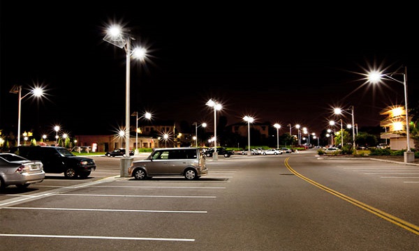
(1) Display and traffic signal display light source. LED lights have the characteristics of shock resistance, fast light response, power saving and long life. They are widely used in various indoor and outdoor displays. They are divided into full-color, three-color and single-color displays. There are more than 100 units nationwide. For development and production. Traffic signal lights mainly use super bright red, green and yellow LEDs. Because the use of LED signal lights is energy-saving and reliable, traffic signal lights are gradually being updated nationwide. At the same time, with the development of urban lighting projects, LEDs are also playing an important role in landscape lights and decoration of urban night landscapes.
(2) Automobile industry. Automotive LEDs include dashboards, audio indicators, switch backlights, reading lights and external brake lights, tail lights, side lights, and headlights. In 1987, my country began to install high-position brake lights on cars. Due to the fast response speed of the LED, the driver can be reminded to brake early, reducing rear-end collisions. In developed countries, central rear-mounted high-position brake lights made of LEDs have become standard parts of automobiles. The LED automotive taillight modules launched by HP in 1996 can be combined into various automotive taillights at will. In addition, the light source in the car dashboard and other various lighting parts can be used as ultra-high brightness luminous lamps, so LED displays are gradually being adopted.
(3) LED backlight. The high-efficiency side-emitting backlight is the most eye-catching. As the backlight source of the liquid crystal screen (LCD), LED has the characteristics of long life, high luminous efficiency, no interference and high cost performance. It has been widely used in electronic watches, mobile phones, electronic calculators and credit card machines. LED is a key component of mobile phones. An ordinary mobile phone or a PHS mobile phone needs about 10 LED devices, while a color screen and a mobile phone with camera function need about 20 LED devices. At this stage, the backlight consumption of mobile phones is very large, and 3.5 billion LED chips are used a year.
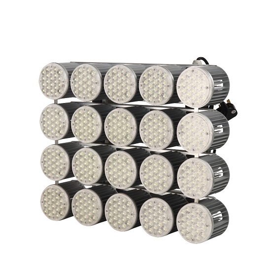
(4) Lighting source. At present, there are few companies that can produce lighting sources. The leading companies are Japan’s Nichia (NICHIA), the United States (CREE), and Europe’s OSRAM (OSRAM). With their original patents, these major manufacturers have monopolized all current white LED cutting-edge technologies, and their products occupy the vast majority of the market. Nichia is the world’s top research and production company for LEDs. For more than ten years, its GaN-based research and development level has been leading other companies for 2 to 3 years.
Semiconductor luminescent material
1.The principle of LED chip light emission.
LED is a component that converts electrical energy into light energy. Its core component is a pn junction made of semiconductor material, which is an electrical injection solid-state light-emitting device. The basic principle is that after a positive bias is applied to the pn junction, the injected minority carriers recombine with the majority carriers, and at the same time the excess energy is released in the form of photons, thereby converting electrical energy into light energy. When a reverse voltage is applied to the pn junction, minority carriers are not injected, so no light is emitted. The essence of its luminescence is that the electron emits photons with energy (E2-E1) during the transition from the high-level excited state (E2) to the low-level ground state (E1), so its light emission is a single wavelength light (infrared or ultraviolet). The two lead frames input direct current, in which the anode rod is connected with the p-type semiconductor, and the cathode rod is connected with the n-type semiconductor. The electrons recombine with the holes on the p-zone semiconductor to emit photons and release excess energy to emit light.
2. Conditions of semiconductor materials.
Through the research on the principle of LED light emission, we conclude that the semiconductor materials used for LED chips must meet the following conditions:
(1) The band gap width is appropriate. When the minority carriers injected by the pn junction emit light with the majority carriers, the released photon energy is less than the band gap width. Therefore, the band gap width of the crystal must be greater than the photon energy of the desired emission wavelength.
(2) P-type and n-type crystals with high conductivity can be obtained. In order to prepare excellent pn junctions, there are two types of p-type and n-type crystals, and the conductivity of these two crystals should be higher.
(3) Obtaining high-quality crystals with good integrity The incompleteness of crystals has a great influence on the luminescence phenomenon. The imperfections mentioned here refer to impurities and lattice defects that can shorten the lifetime of minority carriers and reduce the luminous efficiency. Therefore, obtaining high-quality crystals with good integrity is a necessary condition for making high-efficiency light-emitting diodes [6].
(4) Direct band gap Direct band gap materials are mostly used in the light-emitting field, and have higher luminous efficiency. The mobility of electrons (holes) is higher than that of indirect band gap materials.
3. Selection of semiconductor materials.
At present, wide-gap semiconductor materials III-V compounds and their multi-element mixed crystals are generally used to prepare light-emitting diodes, including: binary compounds GaAs, GaP, GaN, InP, SiC, and ternary compounds GaAsP , AlGaAs, InGaN, AlGaN, InGaP, AIGaP, and quaternary compounds InGaAIP, InGaAsP, etc. The three binary compound luminescent materials currently studied are ZnSe, GaN, and ZnO, which respectively represent the three main research processes of semiconductor luminescent materials.
(1) Zinc selenide (ZnSe). From the perspective of the energy band characteristics of the material, ZnSe was first considered to be a better material for preparing blue-green lasers. However, in the past 40 years, due to the traditional “thermal equilibrium growth” technology, it is difficult to effectively overcome the defects of controlling crystal materials. Problems such as impurities have seriously hindered the development of ZnSe materials. Although the continuous working time of ZnSe-based blue-green semiconductor lasers has been increased from seconds to 400 hours in the past 4 to 5 years, and the working voltage has also been reduced from about 20V to the current 3.7V, it has made considerable progress and development. However, how to obtain p-type doping with high headroom concentration, achieve good low-resistance ohmic contact, extend the service life of the device, and make it practical, there are still a lot of topics to be studied.
(2) Gallium nitride (GaN). Compared with the first and second-generation electronic materials, the third-generation wide-bandgap semiconductor materials have a wider energy gap, a higher saturated electron rate, a larger breakdown voltage, a smaller dielectric constant, and better thermal conductivity. Features. For GaN, its chemical properties are stable, high temperature resistance, and corrosion resistance. It is very suitable for making radiation-resistant, high-frequency, high-power, and high-density integrated electronic devices, as well as blue, green and ultraviolet optoelectronic devices. All these excellent properties have made up for the inherent shortcomings of the first two generations of semiconductor materials. Therefore, GaN materials have been a hot spot of people’s attention in the past 10 years. The rise of gallium nitride as a third-generation semiconductor material is marked by the successful development of high-brightness blue light-emitting diodes and blue lasers. The growth technology and device manufacturing process of GaN have not made substantial progress and breakthroughs in commercial applications until recent years, and GaN currently accounts for the vast majority of the LED market. There are many growth methods for GaN materials. Since the single crystal production process has not yet been resolved, heteroepitaxial growth on the substrate is currently popular. At present, GaN is generally grown on Si, GaAs, sapphire, SiC or other substrate materials.
(3) Zinc oxide (ZnO) Zinc oxide (ZnO) is an alternative material that has been considered to replace GaN in recent years. It is a direct bandgap semiconductor material with a large exciton binding energy (60meV), much greater than that of GaN (26meV), its bandwidth is 3.37eV, and it has a hexagonal wurtzite structure. These advantages make ZnO an excellent material for short-wavelength optoelectronic devices. ZnO is similar to GaN in terms of lattice structure, unit cell parameters, and band gap, and has a higher melting point and greater exciton binding energy than GaN, so it is easy to achieve high efficiency at room temperature or higher Laser emission. ZnO is considered to be a new generation of semiconductor optoelectronic materials. It can not only be used as a substitute for GaN, but also can open up many new application fields and has a very broad application prospect.


