The LED chip is a solid-state semiconductor device. The heart of the LED is a semiconductor wafer. One end of the wafer is attached to a bracket, one end is the negative electrode, and the other end is connected to the positive electrode of the power supply, so that the entire chip is encapsulated by epoxy resin.
The LED chip, also known as the LED light-emitting chip, is the core component of the LED lamp, which is also referred to as the P-N junction.
2. Development process
The basics of how semiconductor materials can generate light have been known for 50 years.
In 1962, Nick Holonyak Jr. of General Electric Company developed the first practical visible light-emitting diode.
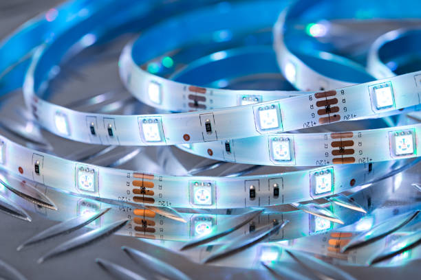
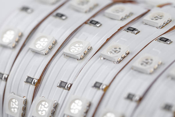
LED is the abbreviation of light emitting diode. Its basic structure is a piece of electroluminescent semiconductor material, which is placed on a leaded shelf, and then sealed with epoxy resin around it, that is, solid package, so it can protect the inner core wire. The role of the LED, so the seismic performance of the LED is good.
At first, LED was used as an indicator light source for instruments and meters. Later, LEDs of various light colors were widely used in traffic lights and large-area display screens, resulting in good economic and social benefits.
Take a 12-inch red traffic light as an example. In the United States, a long-life, low-efficiency 140-watt incandescent lamp is used as the light source, which produces 2,000 lumens of white light.
After the red filter, 90% of the light is lost, leaving only 200 lumens of red light.
In the newly designed lamp, Lumileds used 18 red LED light sources, including circuit losses, a total of 14 watts of power consumption, which can produce the same light effect.
Automotive signal lights are also an important area of application of LED light sources.
3. Working principle
Its main function is to convert electrical energy into light energy, and the main material of the chip is monocrystalline silicon.
The semiconductor wafer consists of two parts, one part is a P-type semiconductor, in which holes dominate, and the other end is an N-type semiconductor, where electrons are mainly.
But when the two semiconductors are connected, a P-N junction is formed between them.
When the current acts on the wafer through the wire, the electrons will be pushed to the P region, where the electrons and holes recombine, and then emit energy in the form of photons, which is the principle of LED light emission.
The wavelength of light, which is also the color of light, is determined by the material that forms the P-N junction.
4. Classification
(1) MB chip
Metal Bonding chip; this chip is a patented product of UEC.
Features:
①The material with high heat dissipation coefficient—Si is used as the substrate. Easy to dissipate heat.
Thermal Conductivity
GaAs: 46 W/m-K
GaP: 77 W/m-K
Si: 125 to 150 W/m-K
Cupper: 300~400 W/m-k
SiC: 490 W/m-K
②The epitaxial layer and the substrate are bonded by the metal layer, and photons are reflected at the same time to avoid the absorption of the substrate.
③ The conductive Si substrate replaces the GaAs substrate, which has good thermal conductivity (the difference in thermal conductivity is 3 to 4 times), and is more suitable for the field of high driving current.
④The bottom metal reflective layer is conducive to the improvement of luminosity and heat dissipation.
⑤ The size can be increased, and it is used in the field of High power.
(2) GB chip
Glue Bonding chip; this chip is a patented product of UEC.
Features:
①The transparent sapphire substrate replaces the light-absorbing GaAs substrate, and its light output is more than twice that of the traditional AS (Absorbable structure) chip, and the sapphire substrate is similar to the GaP substrate of the TS chip.
②The chip emits light on all sides and has an excellent pattern.
③In terms of brightness, its overall brightness has exceeded the level of the TS chip (8.6mil).
④Double-electrode structure, its high current resistance is slightly worse than the definition and characteristics of TS single-electrode TS chip.
(3) TS chip
transparent structure chip, which belongs to HP’s patented product.
Features:
①The chip process is complex, much higher than that of AS LED.
②Excellent reliability.
③Transparent GaP substrate, no light absorption, high brightness.
④ widely used.
(4) AS chip
Absorbable structure chip; After nearly 40 years of development efforts, Taiwan LED optoelectronics industry is in a mature stage for the research and development, production and sales of this type of chip.
The mainland chip manufacturing industry started late, and its brightness and reliability still have a certain gap with the Taiwan industry. The AS chip we are talking about here refers specifically to UEC’s AS chip.
Features:
①The quaternary chip is prepared by the MOVPE process, and the brightness is brighter than that of the conventional chip.
LED lamp beads use low-voltage power supply, and the power supply voltage is between 2-4V, which varies according to different products, so it is a safer power supply than high-voltage power supply, especially suitable for public places;
(2) Current
The working current is 0-15mA, and the brightness becomes brighter as the current increases
(3) Efficiency
It consumes 80% less energy than incandescent lamps with the same light efficiency.
(4) Applicability
Small, each unit LED chip is 3-5mm square, so it can be fabricated into devices of various shapes and suitable for variable environments.
(5) Response time
The response time of its incandescent lamps is milliseconds, and the response time of LED lamps is nanoseconds.
(6) Environmental pollution
No harmful metal mercury.
(7) Color
Changing the current can change the color, and the light-emitting diode can easily adjust the energy band structure and band gap of the material through chemical modification methods, so as to realize multi-color emission of red, yellow, green, blue and orange.
For example, an LED that is red when the current is small, can turn orange, yellow, and finally green as the current increases.
6. Scope of application
LED chips are widely used in lighting, LED large-screen display, traffic lights, decoration, computers, electronic toys gifts, switches, telephones, advertising, urban glory projects and many other production fields.
LED chips are true “green lighting”. In the future of the 21st century, the lighting products with LED as the light source will inevitably replace the white woven lamp and become another revolution in human lighting.
Red light: 9mil regular square, (pure red) wavelength: 620-625nm, up and down 60°, left and right 120°, brightness up to 1000-1200mcd.
Green light: 12mil regular square, (pure green) wavelength: 520-525nm, up and down 60°, left and right 120°, brightness up to 2000-3000mcd.
Performance: It has the characteristics of high brightness, strong anti-static ability, strong anti-decay ability, good consistency, etc. It is the best choice for making LED signs and LED luminous characters.