LED packaging technology is mostly developed and evolved on the basis of discrete device packaging technology. But it is very special. Typically, the die of a discrete device is sealed in a package that protects the die and completes electrical interconnections. The LED package is to complete the output of electrical signals, protect the normal operation of the die, and output the function of visible light. Due to the design and technical requirements of both electrical parameters and optical parameters, it is impossible to simply use the packaging of discrete devices for LEDs.
Product package structure type
Since the 1990s, many breakthroughs have been made in the research and development of LED chips and materials. Trapezoidal structure of transparent substrate, textured surface structure, flip-chip structure, and commercialized ultra-high brightness (above 1cd) red, orange, yellow, green, and blue LED products have come into the market one after another. Since 2000, it has been used in special lighting with low and medium luminous flux.
The upstream and midstream industries of LED have received unprecedented attention, further promoting the downstream packaging technology and industrial development. Various series of products can be produced by using different package structures and sizes, dies of different light-emitting colors and their two-color or three-color combinations.
The type of LED product packaging structure is classified according to the characteristics of light emission color, chip material, light emission brightness, size and so on. A single die generally constitutes a point light source, and a plurality of die assemblies can generally constitute a surface light source and a line light source for information, status indication and display.
Light emitting displays are also constructed using a plurality of dies, through appropriate connections (including series and parallel) of the dies, in combination with suitable optical structures.
For the light-emitting segments and light-emitting points of light-emitting displays, surface-mount LEDs can gradually replace pin-type LEDs. The application design is more flexible, and it has occupied a certain share in the LED display market, and has an accelerated development trend.
Pin Package
The LED pin-type package uses lead frames as the pins of various package shapes. It is the first package structure that has been successfully developed and put on the market. There are many varieties and high technical maturity. In-package structure and reflective layers are still being improved.
Standard LEDs are considered by most customers to be the most convenient and economical solution in the lighting industry today. A typical traditional LED is placed in a package that can withstand 0.1W input power, and 90% of its heat is dissipated from the negative lead frame to the PCB board, and then to the air.
How to reduce the temperature rise of P-N junction
How to reduce the temperature rise of the P-N junction during operation must be considered in packaging and applications. The encapsulation material mostly adopts high temperature curing epoxy resin, which has excellent optical properties, good process adaptability and high product plasticity. It can be made into colored transparent, colorless transparent, colored scattering or colorless scattering lens package.
Different lens shapes make up a variety of shapes and sizes. For example, circles are classified into Φ2mm, Φ3mm, Φ4.4mm, Φ5mm, Φ7mm and so on according to their diameters. Different components of epoxy resin can produce different luminous effects.
Package structure of point light source
There are a variety of different package structures for color point light sources. The ceramic base epoxy package has good operating temperature performance, the pins can be bent into the desired shape, and the volume is small.
The metal base plastic reflector package is an energy-saving indicator light, suitable for power indication.
The flickering type combines the CMOS oscillator circuit chip with the LED die, which can generate flickering light with strong visual impact by itself.
The two-color type consists of two dies of different light-emitting colors, encapsulated in the same epoxy lens, and a third mixed color can be obtained in addition to the two-color. It is widely used in large-screen display systems, and can be packaged to form two-color display devices.
The voltage type combines the constant current source chip and the LED die, which can directly replace various voltage indicators of 5-24V.
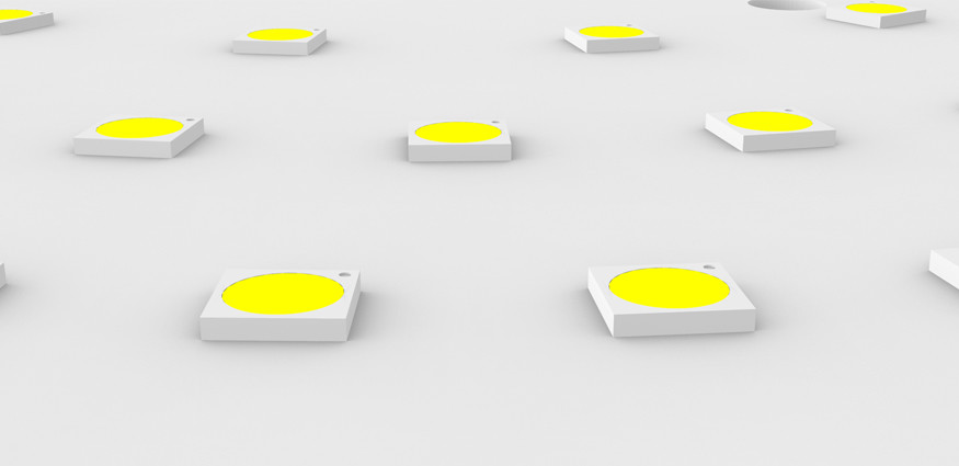
The surface light source is formed by pasting multiple LED dies on the specified position of the PCB board, using a plastic reflective frame cover and potting epoxy resin. The different designs of the PCB board determine the arrangement and connection method of the outer leads, and there are structural forms such as dual in-line and single in-line. Point and area light sources have now developed hundreds of package shapes and sizes for the market and customers.
Surface Mount Package
Advantages of SMD LEDs
In 2002, surface mount packaged LEDs (SMD LEDs) were gradually accepted by the market and gained a certain market share. Switching from lead-type packaging to SMD is in line with the general trend of the entire electronics industry, and many manufacturers have launched such products.
Most of the early SMD LEDs were modified SOT-23 with a transparent plastic body, with an external dimension of 3.04 × 1.11mm, and were packaged with reel-type tape. On the basis of SOT-23, researchers have developed SLM-125 series and SLM-245 series LED with high brightness SMD with lens. The former is single-color emission, and the latter is two-color or three-color emission.
In recent years, SMD LED has become a development hotspot, which has well solved the problems of brightness, viewing angle, flatness, reliability and consistency. With lighter PCB board and reflective layer materials, less epoxy needs to be filled in the display reflective layer. And remove the heavier carbon steel material pins. By reducing the size and reducing the weight, the weight of the product can easily be reduced in half. Ultimately make the application more perfect, especially suitable for indoor and semi-outdoor full-color display applications.
SMD LED common package specifications
Several sizes of common SMD LEDs, and the optimal viewing distance calculated based on the size (plus the necessary clearance) are as follows.
The pad is an important channel for its heat dissipation. The SMD LED data provided by the manufacturer is based on a 4.0 × 4.0 mm pad, which can be designed to be equal to the pad and pin by reflow soldering.
Ultra-high brightness LED products are available in a PLCC (Plastic Leaded Chip Carrier)-2 package with an outline size of 3.0 × 2.8 mm. The high brightness die is assembled by a unique method, and the thermal resistance of the product is 400 K/W. It can be welded by CECC method, and its luminous intensity can reach 1250mcd under 50mA driving current.
The seven-segment one-, two-, three-, and four-digit digital SMD LED display devices feature a character height of 5.08 – 12.7 mm and a wide selection of display sizes.
The PLCC package avoids the manual insertion and pin alignment process required for the pin seven-segment digital display, and meets the production requirements of automatic pick-and-place equipment. The application design space is flexible, and the display is bright and clear.
The multi-color PLCC package features an external reflector that can be easily combined with a light-emitting tube or light guide. Replacing the current transmissive optical design with a reflective type to provide uniform illumination for a large area, develop a power-type SMD LED package that operates under 3.5V, 1A driving conditions.
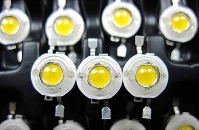
Power Package
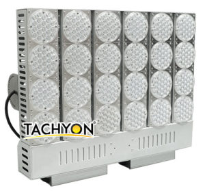
LED chips and packages are developing in the direction of high power. To generate luminous flux 10-20 times larger than Φ5mm LED under high current, effective heat dissipation and non-deteriorating packaging materials must be used to solve the problem of light decay. Therefore, the case and packaging are also its key technologies. LED packages that can withstand several watts of power have emerged. 5W series white, green, blue-green, blue power LEDs have been available since early 2003. The white LED light output reaches 1871m, and the light efficiency is 44.31m/W. Developed LEDs that can withstand 10W of power. The large-area tube measures 2.5 × 2.5mm, operates at 5A, and has a light output of 2001m. There is a lot of room for development as a solid-state lighting source.
In application, the packaged product can be assembled on a metal core PCB board with an aluminum interlayer to form a power density LED. The PCB board is used as the wiring for the connection of the device electrodes, and the aluminum core interlayer can be used as a heat sink to obtain higher luminous flux and photoelectric conversion efficiency.
In addition, the packaged SMDLED is small in size and can be flexibly combined to form a variety of lighting sources such as module type, light guide plate type, concentrating type, and reflection type.
The thermal characteristics of power LEDs directly affect the operating temperature, luminous efficiency, luminous wavelength, and service life of the LED. Therefore, the packaging design and manufacturing technology of power LED chips are even more important.
LED Development and Application Prospects
In recent years, the luminous efficiency of LEDs has increased by 100 times, and the cost has dropped by 80%. Widely used in large-area graphic display full-color screen, status indication, sign lighting, signal display, LCD backlight, and automotive combination taillights and interior lighting, etc.
Its development prospects have attracted global lighting manufacturers to join the LED light source and market development successively. Great development and application prospects are white LEDs. It is economical and environmentally friendly as a solid-state lighting device, and is gradually replacing traditional incandescent lamps. The world’s annual growth rate is more than 20%.
The United States, Japan, Europe and Taiwan Province of China have launched semiconductor lighting programs. At present, the luminous efficiency of ordinary white LED is 100 lm/W. Experts predict that it may exceed 300 lm/W in 2030. The excellent heat dissipation characteristics and optical characteristics of power LEDs are more suitable for the field of general lighting. Academia and industry believe that it is the only way for LEDs to enter the lighting market.
To replace fluorescent lamps, white LEDs must have a luminous efficacy of 250 – 300 lm/W, and the price per Im should be significantly lower than $0.015/Im (current price is about $0.25/Im, red LED is 0.065/Im). To achieve this goal, there are still many technical issues to be studied. But overcoming these problems is not very far away.
According to the principle of solid-state luminescence physics, the luminous efficiency of LED can be approximately 100%. Therefore, LED is known as a new light source in the 21st century, and is expected to become the fourth-generation light source after incandescent lamps, fluorescent lamps, and high-intensity gas discharge lamps.