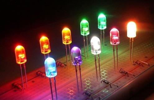
There are generally two forms of point crystal, one is acupuncture, and the other is clipping. People in the industry generally believe that acupuncture is more effective. Therefore, if possible, the orientation of the wafer and the wafer placement surface of the holder should be aligned as much as possible. This can not only ensure the quality, but also improve the speed of spotting.
When the wafer placement surface is inconsistent with the wafer orientation and there is no film turning machine, we can only use clipping. At this time, the operator should pay attention to the strength of holding the clip. If the force of the clip is too large, the semiconductor conductive layer of the wafer may be damaged. This will directly reduce the light-emitting area and affect the light-emitting brightness.
The position of the chip on the chip placement surface of the bracket is also what we need to pay attention to. In particular, the bowl-shaped bracket has better light-emitting and concentrating effects.
Welding Wire
The amount of pressure when welding the wire is also very important. Too little pressure can lead to weak bonding wires, and too much pressure can damage the chip. There is also an important issue here, that is, the length of the wire bonding time, that is to say, the time control of the wire bonding machine. If the welding time is too long, the solder joint may be too large. Since the soldering surface is above the wafer, the size of the area occupied by the solder joint directly affects the size of the light-emitting area. That is to say, the larger the welding surface, the smaller the luminous surface, and the greater the influence of the luminous intensity.
Package
The encapsulation process requires the selection of high-quality potting materials, which should have the following characteristics: (1) No organic solvents, low odor, low toxicity, and safe and hygienic use.
(2) The viscosity is low, the air bubbles can be removed naturally, and it is easy to use.
(3) Room temperature curing, fast curing speed and strong adhesion, generally the curing speed at room temperature is greater than 1h and less than 24h.
(4) The cured product is hard, light and transparent, high gloss, no whitening, and the light transmittance is more than 95%.
(5) Good electrical insulation performance and high withstand voltage. Generally, the volume resistance is greater than 4×10¹⁰Ω, and the breakdown voltage is greater than 10MV.
Different depths of the bracket inserted into the mold strip during packaging will produce different lighting effects.
Imaging calculation formula
Suppose f is the front focal length, f’ is the back focal length, S is the object distance, s’ is the image distance, r is the spherical radius, n is the refractive index of the packaging material, and n’ is the refractive index of the air. We regard the light-emitting point of the chip as a point. So that the coaxial spherical paraxial imaging formula can be approximately quoted:
f’/S’+f/s=l(l)
Then S’=Sf’/S-f.
And f=nr/(nn’)(2)
Then f’=n’r/nn’. (3)
When the package is deep, S<f, it can be known from Eq. 1 that S’ is a negative number. This shows that the image of the chip on the left is a virtual image. And the light emitted by the light-emitting diode is divergent light. The deeper the package, the larger the divergence angle.
When the package is moderate, S=f, it can be known from the formula (1) that s’ is at infinity. It indicates that the light emitted by the light-emitting diode is approximately parallel light.
When the package is shallow, S>f, a real image can be obtained in front of the LED. It can be seen from (1) that when S is slightly larger than f, S-f is very small. S is farther away, the magnification V=S’/S is larger, if S increases, S’ gets closer, and the magnification decreases.
The way of packaging
In general, the package depth is not deep or shallow. And the light emitted by the light-emitting diode is parallel light. However, it is necessary to improve the brightness of the chip, especially when the bracket is bowl-shaped, a shallow package can be appropriately selected. In the same way, it can also be known that the spherical radius r is changed under the same conditions, in order to improve the brightness. For example, when a bullet-shaped mold strip is used, the packaged light-emitting diode can make S>f. So as to obtain an enlarged real image, and the effect of higher brightness than the original bare chip can be obtained.
Avoid air bubbles when encapsulating
In the encapsulation process, a potting material with better quality should be selected. And the air in the potting material should be exhausted before encapsulation. After packaging, there is generally no bubble phenomenon. If bubbles appear, most of them are caused by the gluing process before encapsulation. At this time, the fluidity of the adhesive packaging material is better, and the adhesive action is not easy to be too violent. So that the packaging material is completely adhered around the chip on the bracket as much as possible. With careful operation, air bubbles can be avoided.
Packaging operation process
In addition to the selection of raw materials, the factors that affect the quality of LEDs are very important to directly participate in the operation process of packaging operators. Therefore, it is very necessary to vigorously promote QC management in each process of LED packaging. It is necessary to make each operator clear the essentials of each process before starting his job. And to clarify the stakes between each link and quality. In each process, QC management leaders and supervisors must be set up to inspect the quality of each product one by one and strictly control the quality. Only in this way can each product meet the quality requirements.