Semiconductor light-emitting diodes, referred to as LEDs, have been developed since the 1960s and have gradually become market-oriented, and their packaging technology has also been continuously improved and developed. LEDs have developed from the earliest glass tube packaging to bracket epoxy packaging and surface mount packaging, making low-power LEDs widely used.
Since the 1990s, due to breakthroughs in LED epitaxy and chip technology, quaternary AlGaInP and GaN-based LEDs have come out one after another, realizing full-color LEDs. The luminous brightness is greatly improved, and various colors and white light can be combined. The input power of the device has been greatly improved.
At present, the single-chip 1W high-power LED has been industrialized and introduced to the market, which makes the application of ultra-high-brightness LED continue to expand. First enter the market of special lighting, and move forward to the general lighting market.
Due to the continuous improvement of the input power of LED chips, higher requirements are placed on the packaging technology of these power LEDs. Power LED packaging technology should mainly meet the following two requirements: first, the packaging structure should have high light extraction efficiency, and second, the thermal resistance should be as low as possible. Only in this way can the optoelectronic performance and reliability of the power LED be guaranteed.
Therefore, this article will focus on the introduction and discussion of the packaging technology of power LEDs.
Current Status of Power LED Packaging Technology
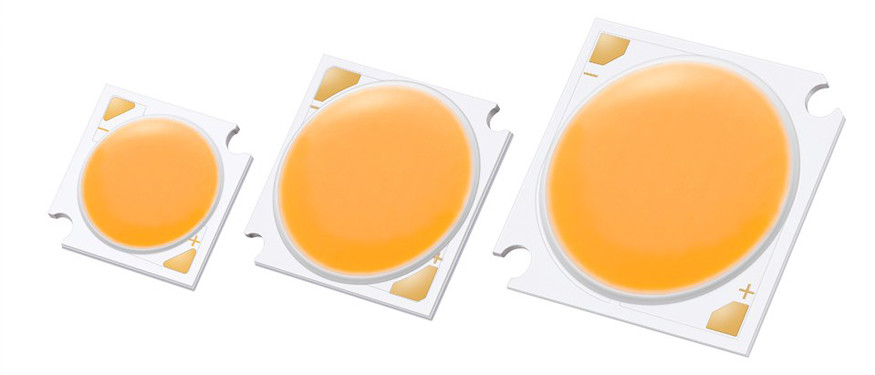
Due to the wide application of power LEDs, the requirements for power LEDs are different in different applications. According to the power, the current power LEDs are divided into ordinary power LEDs and W-class power LEDs. LEDs with input power less than 1W are common power LEDs. LEDs with input power equal to or greater than 1W are W-class power LEDs. There are two common structures of W-class power LEDs, one is a single-chip W-class power LED, and the other is a multi-chip combination of W-class power LEDs.
1. European and American power LED packaging technology:
(1) Ordinary power LED
According to reports, the LED with the “piranha” package structure was first introduced by HP in 1993, called “Super flux LED”. And in 1994, an improved “Snap LED” was introduced. Their typical operating currents are 70mA and 150mA, respectively, with input powers of 0.1W and 0.3W, respectively.
Osram’s “Power TOP LED” is a PLCC package with a metal frame. After that, some other companies introduced a variety of packaging structures for power LEDs. One of the PLCC-4 structure packaging forms, its power is about 200~300mW. The thermal resistance of these structures is generally 75~125°C/W.
In short, the power LEDs of these structures are several times higher than the LEDs in the original bracket package, and the thermal resistance is reduced by about 70% to 80%.
(2) W class power LED
W-class power LEDs are a central part of future lighting. Therefore, major companies in the world have invested a lot of effort in the research and development of W-class power packaging technology, and have applied for various patents for the new structure and new technology obtained.
Single-chip W-class power LEDs were first introduced by Lumileds in 1998 as Luxeon LEDs. The feature of the package structure is that it adopts the form of thermoelectric separation, the flip-chip silicon carrier is directly welded on the heat sink, and new structures and new materials such as reflective cups, optical lenses and flexible transparent glue are used to improve the light extraction of the device. efficiency and improved heat dissipation characteristics. It can work stably and reliably at a large current density, and has a much lower thermal resistance than ordinary LEDs, generally 14~17℃/W.
Existing 1W, 3W and 5W products. The company also recently launched Luxeon III LED products. Due to package and chip improvements, it can operate at higher drive currents. It can maintain 70% lumens after 50,000 hours of operation at 700mA, and 50% of lumens at 1A for 20,000 hours.
2. China’s power LED packaging technology
The post-process packaging capability of ordinary LED products in China is very strong. The variety of packaged products is more complete. According to preliminary estimates, there are more than 200 LED packaging factories nationwide, with a packaging capacity of more than 20 billion pieces per year. The packaging capacity is also very strong, but many packaging factories are private enterprises, and the scale is relatively small at present.
China’s domestic power LED packaging began as early as the 1990s. Some powerful post-package companies started to develop and mass-produce them at that time, such as “piranha” power LEDs. Domestic universities and research institutes rarely conduct research on high-power LED packaging technology. The 13th Research Institute of the Ministry of Information Industry of China has carried out research work on power LED packaging technology and achieved good research results.
Powerful LED packaging companies in China have carried out research and development of power LEDs very early, and achieved good results. Products such as “piranha” and PLCC package structures can be mass-produced, and samples of single-chip 1W high-power LED packages have been developed. It also conducts research and development of high-power LEDs with multi-chip or multi-device combination, and can provide some samples for trial use.
At present, the state has not officially supported the investment in the research and development of high-power LED packaging technology. Domestic research institutes rarely intervene, and packaging companies do not invest enough in R&D (human and financial resources), resulting in a weak domestic development of packaging technology. There is still a considerable gap in the technical level of its packaging compared with foreign countries.
Key Packaging Technology for Power LED Industrialization
Semiconductor LEDs are used as lighting sources, and the luminous flux of conventional products is far away from general-purpose light sources such as incandescent and fluorescent lamps. Therefore, in order to develop LEDs in the field of lighting, the key is to improve their luminous efficiency and luminous flux to the level of existing lighting sources.
The epitaxial material used in power LED adopts MOCVD epitaxial growth technology and multiple quantum well structure. Although its external quantum efficiency needs to be further improved, the biggest obstacle to obtaining high luminous flux is still the low light extraction efficiency of the chip.
The design of the existing power LED adopts a new structure of flip-chip welding to improve the light extraction efficiency of the chip and improve the thermal characteristics of the chip. And by increasing the chip area and increasing the working current, the photoelectric conversion efficiency of the device is improved, thereby obtaining a higher luminous flux.
In addition to the chip, the packaging technology of the device also plays an important role. The key packaging technology processes are as follows.
1. Cooling technology
The traditional indicator-type LED packaging structure is generally made by using conductive or non-conductive glue to mount the chip in a small-sized reflector cup or on a stage, and then encapsulating the device with epoxy resin after completing the internal and external connections of the device with gold wires. Its thermal resistance is as high as 250~300℃/W.
If the new power chip adopts the traditional LED package, the junction temperature of the chip will rise rapidly and the epoxy carbon will turn yellow due to poor heat dissipation, which will cause the accelerated light decay of the device until it fails. It even fails due to the open circuit caused by the stress generated by the rapid thermal expansion.
Therefore, for a power LED chip with a large working current, a new package structure with low thermal resistance, good heat dissipation and low stress is the technical key of the power LED device. The chips are bonded with materials with low resistivity and high thermal conductivity. A copper or aluminum heat sink is added to the lower part of the chip, and a semi-encapsulated structure is used to accelerate heat dissipation. Even a secondary heat sink is designed to reduce the thermal resistance of the device.
The inside of the device is filled with flexible silicone rubber with high transparency. Within the temperature range of the silicone rubber (usually -40°C~200°C), the colloid will not cause the device to open due to sudden temperature changes, nor will it turn yellow. Phenomenon. R&D personnel should also fully consider the thermal conductivity and heat dissipation characteristics of the part material to obtain good overall thermal characteristics.
2. Secondary optical design technology
In order to improve the light extraction efficiency of the device, an additional reflector cup and multiple optical lenses are designed.
3. Power LED white light technology
There are three common process methods for realizing white light:
1) Coat the blue chip with YAG phosphor. The blue light of the chip excites the phosphor to emit yellow-green light with a typical value of 500nm~560nm, and the yellow-green light and the blue light synthesize white light. The method is relatively simple to prepare, has high efficiency and is practical. The disadvantage is that the consistency of the glue amount is poor, the phosphor powder is easy to precipitate, resulting in poor uniformity of the light-emitting surface and poor color tone consistency. Color temperature is high. Color rendering is not ideal.
2) Multiple chips or multiple devices of RGB three primary colors emit light and mix colors into white light. Or use blue + yellow-green dual-chip complementary colors to generate white light. As long as the heat dissipation is good, the white light generated by this method is more stable than the previous method, but the driving is more complicated. In addition, the researchers also need to consider the different light decay speeds of different color chips.
3) Coat the RGB phosphor on the UV chip. Using violet light to excite phosphors to generate white light by mixing three primary colors. However, the current ultraviolet light chips and RGB phosphors have low efficiency, and epoxy resins are easily decomposed and aged under ultraviolet light irradiation.
We believe that the industrialization of W-class power LED products for lighting must also solve the following technical problems:
①Powder coating amount control:
The glue coating method used in the LED chip + phosphor process is usually to mix the phosphor and glue and then apply it to the chip with a dispenser. During the operation, it is difficult to control the uniformity of the coating amount of the phosphor in this process because the viscosity of the carrier glue is a dynamic parameter, the specific gravity of the phosphor is larger than that of the carrier glue and the precipitation occurs, and the accuracy of the dispenser is difficult. This results in uneven color of white light.
②Chip photoelectric parameter coordination:
The characteristics of the semiconductor process determine that there may be differences in optical parameters (such as wavelength, light intensity) and electrical parameters (such as forward voltage) between the same material and the same wafer chip. The RGB three-primary color chip is even more so, which has a great influence on the chromaticity parameters of white light. This is one of the key technologies that industrialization must solve.
③Light chromaticity parameter control according to application requirements:
Products with different uses have different requirements for the color coordinates, color temperature, color rendering, optical power (or light intensity) and spatial distribution of light of white LEDs. The control of the above parameters involves the coordination of various factors such as product structure, process methods, and materials. In industrial production, it is very important to control the above factors to obtain products that meet the application requirements and have good consistency.
4. Testing technology and standards
With the development of W-class power chip manufacturing technology and white LED process technology, LED products are gradually entering the (special) lighting market. The traditional LED product parameter detection standards and test methods for display or indication can no longer meet the needs of lighting applications. Semiconductor equipment and instrument manufacturers have also launched their own test instruments. There are certain differences in the test principles, conditions and standards used by different instruments, which increases the difficulty of test applications and product performance comparison and complicates problems.
5. Screening technology and reliability guarantee
Due to the limitation of the appearance of the luminaire, the assembly space of the LED for lighting is sealed and limited. Sealed and limited space is not conducive to LED heat dissipation, which means that the use environment of lighting LEDs is inferior to traditional LED products for display and indication.
In addition, lighting LEDs work under high current drive, which puts forward higher reliability requirements. In industrial production, it is necessary to formulate appropriate thermal aging, temperature cycle impact, load aging process screening tests for different product uses, to eliminate early failure products, and to ensure product reliability.
6. Electrostatic protection technology
The positive and negative electrodes of the blue chip on the sapphire substrate are both located on the chip with a small distance. For the InGaN/AlGaN/GaN double heterojunction, the activated thin layer of InGaN is only a few tens of nanometers, which has little resistance to static electricity, and is easily broken down by static electricity, causing the device to fail. Therefore, in industrial production, whether the prevention of static electricity is appropriate will directly affect the yield, reliability and economic benefits of the product.