LED is a type of light-emitting device that can directly convert electrical energy into visible light and radiant energy. It has low operating voltage, low power consumption, high luminous efficiency, extremely short luminous response time, pure light color, firm structure, impact resistance, and vibration resistance. , stable and reliable performance, light weight, small size, low cost and a series of characteristics.
With rapid development, it is now able to mass-produce high-brightness, high-performance products in various colors throughout the visible spectrum. The domestic production of red, green, orange and yellow LEDs accounts for about 12% of the world’s total. The industrial goal in the next five years is to achieve an annual output of 30 billion LEDs, and to achieve large-scale production of ultra-bright AiGslnP LED epitaxial wafers and chips . With an annual output of more than 1 billion red, orange, and yellow ultra-high-brightness LED dies, it has broken through the key technology of GaN materials and achieved medium-volume production of blue, green, and white LEDs.
It is predicted that by 2025, the international LED market demand will be about 200 billion, and the sales will reach 150 billion US dollars.
In the LED industry link, the upstream is LED substrate wafer and substrate production, the midstream industrialization is LED chip design and manufacturing, and the downstream is LED packaging and testing. The development of packaging technology with low thermal resistance, excellent optical properties, and high reliability is the only way for the industrialization of new LEDs to become practical and market. In a sense, it is the link between the industry and the market. Only when the package is packaged can it become a terminal product, put into practical application, and provide services to customers, so that the industry chain is interlinked and seamless.
2. The Particularity of LED Packaging
LED packaging technology is mostly developed and evolved on the basis of discrete device packaging technology, but it has great particularity. Typically, the die of a discrete device is sealed in a package that protects the die and completes electrical interconnections. The LED package is to complete the output of electrical signals to protect the normal output of the die. The function of visible light has both electrical parameters and design and technical requirements of optical parameters, so it is impossible to simply use the packaging of discrete devices for LEDs.
Structural features
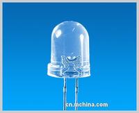
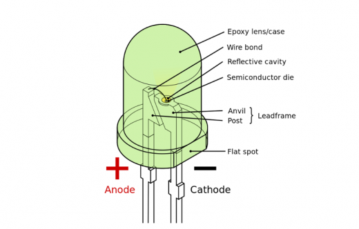
The conventional Φ5mm LED package is to bond or sinter a square die with a side length of 0.25mm on a lead frame. The positive electrode of the die is connected to the gold wire through the ball contact point, and the inner lead is bonded to one pin, and the negative electrode is connected to the other pin of the lead frame through the reflector cup, and then the top is encapsulated with epoxy resin.
The function of the reflector cup is to collect the light emitted from the side and interface of the die and emit it in the desired direction angle. The top encapsulated epoxy is shaped into a shape. There are several functions:
Protect the die, etc. from external erosion.
Using different shapes and material properties (with or without dispersing agent), it functions as a lens or a diffusing lens to control the divergence angle of light.
Refractive index
The refractive index of the die is too closely related to the refractive index of the air, so that the critical angle of total reflection inside the die is very small, and only a small part of the light generated by the active layer is taken out, and most of it is easily reflected inside the die.
Absorption, prone to total reflection resulting in excessive light loss. The epoxy resin with the corresponding refractive index is selected as the transition to improve the light output efficiency of the die.
The epoxy resin used to form the tube shell must have moisture resistance, insulation, mechanical strength, and high refractive index and transmittance to the light emitted by the tube core. Selecting packaging materials with different refractive indices, the effects of packaging geometry on the photon escape efficiency are different. The angular distribution of luminous intensity is also related to the structure of the die, the way of light output, and the material and shape of the encapsulated lens. If a pointed resin lens is used, the light can be concentrated in the axial direction of the LED, and the corresponding viewing angle is small. If the top resin lens is circular or flat, its corresponding viewing angle will be increased.
The effect of temperature on LED performance
Under normal circumstances, the luminous wavelength of LED changes with temperature to 0.2-0.3nm/℃, and the spectral width increases accordingly, which affects the color vividness. In addition, when forward current flows through the p-n junction, thermal losses cause the junction temperature to rise. In the vicinity of room temperature, the luminous intensity of the LED will correspondingly decrease by about 1% for every 1°C increase in temperature.
It is important to maintain color purity and luminous intensity as the package dissipates heat. In the past, the method of reducing its driving current was used to reduce the junction temperature, and the driving current of most LEDs was limited to about 20mA. However, the light output of LEDs increases with increasing current. At present, the driving current of many power LEDs can reach 70mA, 100mA or even 1A.
It is necessary to improve the packaging structure, a new LED packaging design concept and low thermal resistance packaging structure and technology to improve thermal characteristics. For example, a large-area chip flip-chip structure is used, silver paste with good thermal conductivity is used, the surface area of the metal bracket is increased, and the silicon carrier of the solder bump is directly mounted on the heat sink. In addition, in the application design, the thermal design and thermal conductivity of the PCB circuit board are also very important.
development trend
After entering the 21st century, the high-efficiency, ultra-high brightness and full-color LEDs continue to develop and innovate. The light efficiency of red and orange LEDs has reached 100Im/W, and the green LED is 501m/W. The luminous flux of a single LED also reaches tens of Im. LED chips and packages no longer follow Gong’s traditional design concepts and manufacturing production models.
In terms of increasing the light output of chips, R&D is not limited to changing the amount of impurities, lattice defects and dislocations within the material to improve internal efficiency. At the same time, how to improve the internal structure of the die and package? How to enhance the probability of photon output inside the LED and improve the light efficiency? How to solve the optimization design of heat dissipation, light extraction and heat sink? How to improve optical performance and accelerate the process of surface mount SMD? These issues are the mainstream direction of R&D in the industry.
3. Product Package Structure Type
Since the 1990s, many breakthroughs have been made in the research and development of LED chips and materials. Trapezoidal structure of transparent substrate, textured surface structure, flip-chip structure, and commercialized ultra-high brightness (above 1cd) red, orange, yellow, green, and blue LED products have come into the market one after another. Since 2000, it has been used in special lighting with low and medium luminous flux. The upstream and midstream industries of LED have received unprecedented attention, further promoting the downstream packaging technology and industrial development. Using different packaging structures and sizes, different luminous colors of the die and its two-color or three-color combination, it can produce a variety of series, varieties, and specifications of products.
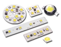
The type of LED product packaging structure is classified according to the characteristics of light emission color, chip material, light emission brightness, size and so on. A single die generally constitutes a point light source, and a plurality of die assemblies can generally constitute a surface light source and a line light source for information, status indication and display. The light-emitting display is also composed of a plurality of dies, which are combined with suitable optical structures through appropriate connection (including series and parallel) of the dies, to form the light-emitting segments and light-emitting points of the light-emitting display.
Surface-mount LEDs can gradually replace pin-type LEDs, and the application design is more flexible. It has occupied a certain share in the LED display market and has an accelerated development trend. Some solid-state lighting source products are listed, which will become the medium and long-term development direction of LED in the future.
4-Pin Package
pin package
The LED pin-type package uses a lead frame as the pins of various package shapes. It is the first package structure that has been successfully developed and put on the market. There are many varieties and high technical maturity. In-package structure and reflective layers are still being improved.
Standard LEDs are considered by most customers to be the most convenient and economical solution in the display industry today. A typical traditional LED is placed in a package that can withstand 0.1W input power, and 90% of its heat is dissipated from the negative lead frame to the PCB board, and then to the air.
How to reduce the temperature rise of the pn junction during operation must be considered in packaging and applications. Most of the encapsulation materials use high temperature curing epoxy resin, which has excellent optical properties, good process adaptability and high product reliability. Can be made into colored transparent or colorless transparent and colored scattering or colorless scattering lens package.
Different lens shapes make up a variety of shapes and sizes. For example, the circle is divided into Φ2mm, Φ3mm, Φ4.4mm, Φ5mm, Φ7mm and so on according to the diameter. Different components of epoxy resin can produce different luminous effects.
Package structure of point light source
There are many different package structures for the color point light source: the ceramic base epoxy resin package has better operating temperature performance, the pins can be bent into the desired shape, and the volume is small.
The metal base plastic reflector package is an energy-saving indicator light, suitable for power indication.
The flickering type combines the CMOS oscillator circuit chip with the LED die, which can generate flickering light with strong visual impact by itself.
The two-color type is composed of two dies with different light-emitting colors, which are encapsulated in the same epoxy lens. In addition to the two-color, a third mixed color can be obtained. It is widely used in large-screen display systems and can be packaged to form Two-color display device.
The voltage type combines the constant current source chip and the LED die, which can directly replace various voltage indicators of 5-24V.
The surface light source is formed by bonding multiple LED dies on the specified positions of the micro PCB board, using a plastic reflective frame cover and potting epoxy resin. The different designs of the PCB board determine the arrangement and connection method of the outer leads, and there are structural forms such as dual in-line and single in-line. Point and area light sources have now developed hundreds of package shapes and sizes for the market and customers.
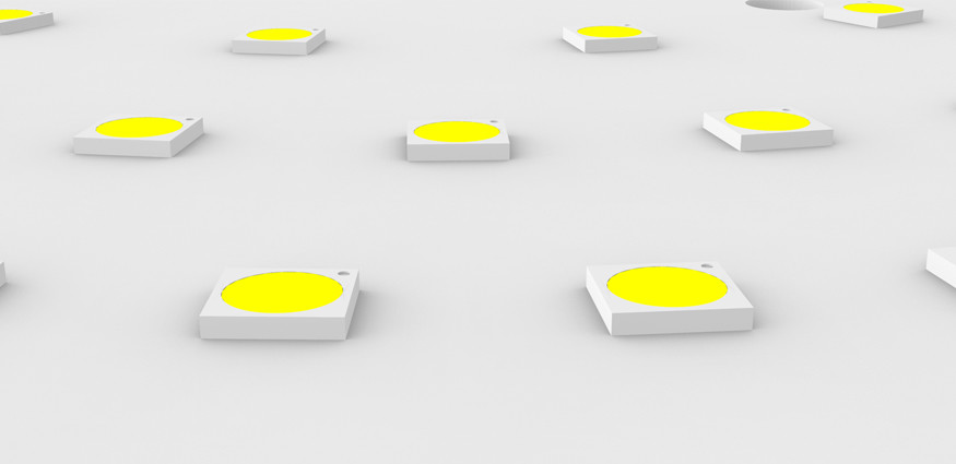
5. Surface Mount Packages
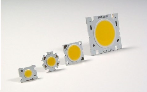
In 2002, surface mount packaged LEDs (SMD LEDs) were gradually accepted by the market and gained a certain market share. The shift from lead-based packaging to SMD is in line with the general trend of the entire electronics industry, with many manufacturers launching such products.
Most of the early SMD LEDs used a modified SOT-23 with a transparent plastic body. Dimensions 3.04 × 1.11mm, reel type container tape packaging. On the basis of SOT-23, SLM-125 series and SLM-245 series LED with high brightness SMD with lens are developed. The former is single-color emission, and the latter is two-color or three-color emission.
In recent years, SMD LED has become a development hotspot, which has well solved the problems of brightness, viewing angle, flatness, reliability and consistency. With lighter PCB board and reflector material, less epoxy needs to be filled in the display reflector, and the heavier carbon steel pins are removed. By reducing size and weight, the weight of the product can easily be cut in half, resulting in a perfect application. Especially suitable for indoor and semi-outdoor full-color display applications.