High-power LED packaging has been a research hotspot in recent years due to its complex structure and process, which directly affects the performance and life of LEDs. In particular, high-power white LED packaging is a hot spot in research hotspots.
The functions of the LED package mainly include:
Mechanical protection to improve reliability.
Strengthen heat dissipation to reduce chip junction temperature and improve LED performance.
Optical control to improve light output efficiency and optimize beam distribution.
Power supply management, including AC/DC conversion, and power control, etc.
The selection of LED packaging methods, materials, structures and processes is mainly determined by factors such as chip structure, optoelectronic/mechanical properties, specific applications and costs.
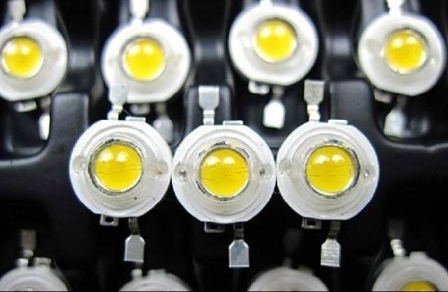
After more than 40 years of development, LED packaging has experienced development stages such as bracket type, SMD type, and power LED. With the increase of chip power, especially the demand for the development of solid-state lighting technology, new and higher requirements are put forward for the optical, thermal, electrical and mechanical structures of LED packaging.
In order to effectively reduce the thermal resistance of the package and improve the light extraction efficiency, a new technical idea must be adopted for the package design.
Key Technologies of High-power LED Packaging
High-power LED packaging mainly involves light, heat, electricity, structure and technology. These factors are both independent of each other and affect each other. Among them, light is the purpose of LED packaging, heat is the key, electricity, structure and technology are the means, and performance is the specific embodiment of the packaging level.
In terms of process compatibility and reducing production costs, LED package design should be carried out at the same time as chip design, that is, the package structure and process should be considered during chip design. Otherwise, after the chip manufacturing is completed, the chip structure may be adjusted due to the need for packaging, thereby prolonging the product development cycle, increasing the process cost, and sometimes even impossible.
Specifically, the key technologies of high-power LED packaging include:
(1) Low thermal resistance packaging process
For the existing LED light efficiency level, about 80% of the input electrical energy is converted into heat. And LED chip area is small, therefore, chip heat dissipation is a key problem that LED packaging must solve. It mainly includes chip layout, packaging material selection (substrate material, thermal interface material) and process, heat sink design, etc.
LED package thermal resistance mainly includes internal thermal resistance and interface thermal resistance of materials (heat dissipation substrate and heat sink structure). The function of the heat dissipation substrate is to absorb the heat generated by the chip and conduct it to the heat sink to achieve heat exchange with the outside world. Commonly used heat dissipation substrate materials include silicon, metals (such as aluminum, copper), ceramics (such as Al2O3, AlN, SiC) and composite materials.
Low-temperature co-fired ceramic metal substrate technology firstly prepares high-power LED chips and corresponding ceramic substrates suitable for eutectic welding, and then directly welds the LED chips and substrates together. Because the eutectic solder layer, electrostatic protection circuit, driving circuit and control compensation circuit are integrated on the substrate, not only the structure is simple, but also the heat dissipation performance is greatly improved due to the high thermal conductivity of the material and less thermal interface. This presents a solution for high-power LED array packaging.
The effect of package interface on thermal resistance
Studies have shown that the package interface also has a large impact on thermal resistance. If the interface is not handled properly, it is difficult to obtain good heat dissipation. For example, an interface with good contact at room temperature may have interfacial gaps at high temperature, and warpage of the substrate may also affect bonding and local heat dissipation.
The key to improving LED packaging is to reduce interface and interface contact thermal resistance and enhance heat dissipation. Therefore, the choice of thermal interface material (TIM) between the chip and the heat sink substrate is very important.
The commonly used TIMs for LED packaging are conductive adhesives and thermally conductive adhesives. Due to the low thermal conductivity, generally 0.5-2.5W/mK, the interface thermal resistance is very high. The use of low-temperature or eutectic solder, solder paste, or conductive adhesive doped with nanoparticles as the thermal interface material can greatly reduce the interface thermal resistance.
(2) High light extraction rate package structure and process
Loss of Photon Radiation
During the use of LEDs, the loss of photons generated by radiation recombination when emitted outward mainly includes three aspects, namely, the internal structural defects of the chip and the absorption of materials, the reflection loss of photons at the exit interface due to the difference in refractive index, And the total reflection loss due to the incident angle being larger than the critical angle of total reflection. Therefore, a lot of light cannot be emitted from the chip to the outside.
The way of high light extraction rate
By coating a transparent adhesive layer with a relatively high refractive index on the surface of the chip, since the adhesive layer is located between the chip and the air, the loss of photons at the interface is effectively reduced, and the light extraction efficiency is improved. In addition, the role of the potting compound also includes mechanical protection of the chip, stress relief, and as a light guide structure. Therefore, the industry requires high light transmittance, high refractive index, good thermal stability, good fluidity, and easy spraying.
How to improve package reliability
In order to improve the reliability of LED packaging, it is necessary to require the potting compound to have the characteristics of low moisture absorption, low stress, and aging resistance. Currently commonly used potting compounds include epoxy resin and silicone. Silica gel is obviously superior to epoxy resin due to its high light transmittance, high refractive index, good thermal stability, low stress and low hygroscopicity. It is widely used in high-power LED packaging, but the cost is high.
Studies have shown that increasing the refractive index of silica gel can effectively reduce the photon loss caused by the physical barrier of the refractive index and improve the external quantum efficiency. However, the performance of silica gel is greatly affected by the ambient temperature. As the temperature increases, the thermal stress inside the silica gel increases, resulting in a decrease in the refractive index of the silica gel, thereby affecting the LED light efficiency and light intensity distribution.
Effect of phosphors on light rate
The function of phosphor is to combine light and color to form white light. Its characteristics mainly include particle size, shape, luminous efficiency, conversion efficiency, stability (thermal and chemical) and so on. Among them, luminous efficiency and conversion efficiency are the key.
Studies have shown that as the temperature rises, the quantum efficiency of the phosphor decreases, the light output decreases, and the radiation wavelength also changes, resulting in changes in the color temperature and chromaticity of white LEDs.
Higher temperatures also accelerate phosphor aging. The reason is that the phosphor coating is made of epoxy or silica gel and phosphor, and the heat dissipation performance is poor. When irradiated by violet light or ultraviolet light, it is prone to temperature quenching and aging, which reduces the luminous efficiency.
In addition, the thermal stability of the encapsulant and phosphors at high temperatures is also problematic. Since the size of commonly used phosphors is above 1um, the refractive index is greater than or equal to 1.85, while the refractive index of silica gel is generally around 1.5. Due to the mismatch of the refractive indices between the two, and the size of the phosphor particles is much larger than the light scattering limit (30nm), there is light scattering on the surface of the phosphor particles, which reduces the light extraction efficiency.
By doping the nano-phosphor in the silica gel, the refractive index can be increased to above 1.8, the light scattering can be reduced, the LED light extraction efficiency can be improved (10%-20%), and the light color quality can be effectively improved.