From a practical application point of view: high-power LED devices that are simple to install and use and relatively small in size will definitely replace traditional low-power LED devices in most lighting applications.
The benefits are very obvious. In order to meet the needs of lighting, the lighting fixture composed of low-power LEDs must concentrate the light energy of many LEDs to meet the design requirements. The disadvantage is that the circuit is very complicated and the heat dissipation is not smooth. In order to balance the current-voltage relationship between the individual LEDs, engineers must design complex power supply circuits.
In contrast, the power of a single high-power LED is much larger than that of a single LED, which is equal to the sum of several low-power LEDs. The power supply circuit is relatively simple, the heat dissipation structure is perfect, and the physical characteristics are stable. Therefore, it is inevitable for high-power LED devices to replace low-power LED devices to become mainstream semiconductor lighting devices.
However, for the packaging method of high-power LED devices, we cannot simply apply the packaging methods and packaging materials of traditional low-power LED devices. Large power dissipation, large heat generation, and high light extraction efficiency put forward new and higher requirements for our packaging process packaging equipment and packaging materials.
2. High-power LED Chip
In order to obtain high-power LED devices, suitable high-power LED chips must be prepared. There are several common manufacturing methods in the world.
2.1 Oversize method:
By increasing the effective light-emitting area and size of a single LED, the electrode structure (usually a comb-shaped electrode) is specially designed to promote the uniform distribution of the current flowing through the TCL layer to achieve the expected luminous flux. However, simply increasing the light emitting area cannot solve the fundamental heat dissipation and light output problems, and cannot achieve the expected luminous flux and practical application effects.
2.2 Silicon backplane flip-chip method:
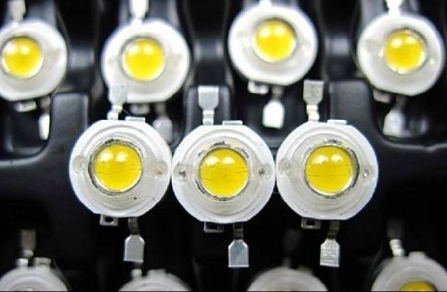
First, a large-size LED chip (Flip Chip LED) with electrodes suitable for eutectic welding was prepared. At the same time, a silicon base plate of corresponding size is prepared, and a gold conductive layer and a lead-out conductive layer (ultrasonic gold wire ball bonding point) for eutectic bonding are fabricated on it. Then, use eutectic bonding equipment to bond the large-sized LED chips to the silicon substrate. Such a structure is more reasonable, considering both the problem of light emission and the problem of heat dissipation. This is the current mainstream High Output Power Chip LED production method.
American LumiLeds company developed an AlGaInN power flip-chip (FCLED) structure in 2001. The specific method is:
In the first step, a NiAu layer with a thickness greater than 500A is deposited on the P-type GaN:Mg on top of the epitaxial wafer for ohmic contact and back reflection.
In the second step, the P-type layer and the multiple quantum well active layer are selectively etched away using a mask to expose the N-type layer.
The third step is to deposit and etch to form an N-type ohmic contact layer, the chip size is 1×1 mm2, the P-type ohmic contact is square, and the N-type ohmic contact is inserted in a comb shape. This shortens the current spreading distance and minimizes spreading resistance.
In the fourth step, the metallized bumped AlGaInN chip is flip-chip bonded to a silicon carrier with ESD protection diodes (ESD).
2.3 Flip-chip method of ceramic bottom plate:
First, an LED chip with a large light-emitting area suitable for the eutectic welding electrode structure and a corresponding ceramic base plate are prepared by using the general equipment of the LED wafer factory, and the eutectic welding conductive layer and the lead-out conductive layer are made on the top. Afterwards, the large-sized LED chips and the ceramic base plate are welded together using eutectic welding equipment.
Such a structure considers the problem of light emission and heat dissipation, and the ceramic bottom plate used is a high thermal conductivity ceramic plate, and the effect of heat dissipation is very ideal. The price is relatively low. Therefore, it is a more suitable base material at present, and can reserve installation space for the future integrated circuit integrated package servo circuit.
2.4 Sapphire substrate transition method:
After the PN junction is grown on the sapphire substrate according to the traditional InGaN chip manufacturing method, the sapphire substrate is cut off, and then the traditional quaternary material is connected to manufacture a large-size blue LED chip with an upper and lower electrode structure.
Cree Corporation of the United States is the only manufacturer in the world that uses SiC substrate to manufacture AlGaInN ultra-high brightness LEDs. Over the past few years, the AlGaInN/SiCa chip structure has been continuously improved, and the brightness has been continuously improved. Since the P-type and N-type electrodes are second only to the bottom and top of the chip respectively, single-wire bonding has good compatibility and is easy to use. Therefore, it has become another mainstream in the development of AlGaInN LEDs.
3. Basic Packaging Structure
There are two main issues to be considered in high-power LED packaging: heat dissipation and light output.
3.1 Heat dissipation coefficient
No.
Material
Thermal conductivity/λW (m.K)
1
Carbon steel
(C=0.5-1.5) 39.2-36.7
2
Nickel steel
(Ni=1%-50%) 45.5-19.6
3
Brass
(70Cu-30Zn) 109
4
Aluminum alloy
(60Cu-40Ni) 22.2
5
Aluminum alloy
(87Al-13Si) 162
6
Aluminum bronze
(90Cu-10Al) 56
7
Magnesium
156
8
Molybdenum
138
9
Platinum
71.4
10
silver
427
11
Tin
67
12
Zinc
121
13
Pure copper
398
14
Gold
315
15
Pure aluminum
236
16
Pure iron
81.1
17
Glass
0.65-0.71
From the current/temperature/luminous flux graph, it can be seen that heat dissipation is critical for power LED devices. If the heat generated by the current cannot be dissipated in time and the junction temperature of the PN junction is kept within the allowable range, stable light output and normal device life will not be maintained.
It can be seen from Table 1 that the thermal conductivity of silver is the best among the commonly used heat dissipation materials, but the cost of the silver conductive heat dissipation plate is high and it is not suitable for general-purpose heat sinks. The thermal conductivity of copper is close to that of silver, and its cost is lower than that of silver. Although the thermal conductivity of aluminum is lower than that of copper, the advantage is that the overall cost is the lowest, which is conducive to large-scale manufacturing.
After two years of experiments and comparisons, we found that it is more appropriate to use a copper-based or silver-based heat sink to connect the chip, and then connect the heat sink to an aluminum-based heat sink with a stepped thermal conductivity structure. Thermal conductivity efficiently transfers the heat generated by the chip to the aluminum-based heat sink, and then dissipates the heat through the aluminum-based heat sink (through air cooling or thermal conduction).
Selection of heat sink material
The advantage of this approach is: fully consider the performance-price ratio of the radiator, combine radiators with different characteristics to achieve efficient heat dissipation, and rationalize cost control.