Film printed circuit
This kind of film circuit is generally printed on PET with silver paste. There are two process methods for pasting and pasting electronic components on this kind of film circuit. One is the traditional process method, which is the 3-glue method (red rubber, silver rubber, encapsulation rubber) or the 2-glue method (silver rubber, encapsulation Glue), another so-called new process is the 1-glue method—as the name suggests, one glue can be used to paste and paste electronic components instead of 3 glues or 2 glues. The key to this new process is to use a new type of conductive adhesive, which has the conductivity and process performance of solder paste; when used, it is fully compatible with the current SMT brushing solder paste operation method without any additional equipment.
How to Choose SMT
Overview
The selection and design of surface-mounted components is a key part of the overall product design. The designer determines the electrical performance and function of the components in the system structure and detailed circuit design stage. In the SMT design stage, it should be based on the specific conditions and overall situation of the equipment and process. The design requirements determine the packaging form and structure of surface mount components. Surface-mounted solder joints are both mechanical connection points and electrical connection points. A reasonable choice will have a decisive impact on improving PCB design density, productivity, testability and reliability.
There is no difference in function between surface-mounted components and plug-in components. The difference lies in the packaging of the components. Surface-mounted packages must withstand high temperature resistance during soldering. Components and substrates must have matching coefficients of thermal expansion. These factors must be fully considered in product design.
The main advantages of choosing the right package are:
1) Effectively save PCB area;
2) Provide better electrical performance;
3) Protect the interior of the components from environmental influences such as humidity;
4) Provide good communication links;
5) Help dissipate heat and provide convenience for transmission and testing.
Selection of surface mount components
Surface mount components are divided into two categories: active and passive. According to the shape of the pin, it is divided into gull wing type and “J” type. The following describes the selection of components in this category.
Passive components
Passive devices mainly include monolithic ceramic capacitors, tantalum capacitors, and thick film resistors, with a rectangular or cylindrical shape. Cylindrical passive components are called “MELF”. They are prone to rolling when reflow soldering. Special pad design is required and should generally be avoided. Rectangular passive components are called “CHIP” chip components. They are small in size, light in weight, antimicrobial impact and shock resistance, and low parasitic loss. They are widely used in various electronic products. In order to obtain good solderability, the electroplating of the nickel barrier layer must be selected.
Active device
There are two main types of surface mount chip carriers: ceramics and plastics.
The advantages of ceramic chip packaging are:
1) Good airtightness and good protection for the internal structure;
2) The signal path is shorter, and the parasitic parameters, noise, and delay characteristics are significantly improved;
3) Reduce power consumption.
The disadvantage is that because the leadless absorbs the stress generated when the solder paste melts, the CTE mismatch between the package and the substrate can cause solder joints to crack during soldering. The most commonly used ceramic wafer carrier is the leadless ceramic wafer carrier LCCC.
Plastic packaging is widely used in the production of military and civilian products, and has a good cost performance. Its packaging forms are divided into: small outline transistor SOT; small outline integrated circuit SOIC; plastic package leaded chip carrier PLCC; small outline J package; plastic flat package PQFP.
In order to effectively reduce the PCB area, SOIC with less than 20 pins, PLCC with 20-84 pins, and PQFP with more than 84 pins are preferred when the device functions and performance are the same.
How to reduce failures
The manufacturing process, handling, and printed circuit assembly (PCA) testing all subject the package to a lot of mechanical stress, which can cause failure. As the grid array package becomes larger and larger, how to set the security level for these steps becomes more and more difficult.
For many years, the monotonic bending point test method is a typical feature of the package. The test is described in IPC/JEDEC-9702 “Monotonic Bending Characteristics of Board Level Interconnects”. This test method describes the breaking strength of the horizontal interconnection of printed circuit boards under bending load. However, this test method cannot determine the maximum allowable tension.
For the manufacturing process and assembly process, especially for lead-free PCA, one of the challenges it faces is the inability to directly measure the stress on the solder joints. The most widely used metric used to describe the risk of interconnected components is the tension of the printed circuit board adjacent to the component, which is described in IPC/JEDEC-9704 “Printed Wiring Board Strain Test Guidelines”.
A few years ago, Intel realized this problem and began to develop a different testing strategy to reproduce the worst bending situation in practice. Other companies such as Hewlett-Packard also realized the benefits of other testing methods and began to consider similar ideas to Intel. As more and more chip manufacturers and customers realize that the determination of the tension limit used to minimize mechanical failures during manufacturing, handling and testing is of great value, this method has caused more and more attentions. interest.
As the use of lead-free equipment expands, users are more and more interested; because many users are facing quality problems.
With the increase of interest from all parties, IPC feels it is necessary to help other companies develop various test methods that can ensure that BGAs are not damaged during manufacturing and testing. This work is jointly carried out by the IPC 6-10d SMT Attachment Reliability Test Method Working Group and the JEDEC JC-14.1 Packaged Equipment Reliability Test Method Subcommittee, and the work has been completed.
The test method specifies eight contact points arranged in a circular array. The PCA with a BGA in the center of the printed circuit board is placed in such a way that the component is mounted face down on the support pins, and the load is applied to the back of the BGA. Place the strain gauge adjacent to the part according to the recommended gauge layout of IPC/JEDEC-9704.
The PCA will be bent to the relevant tension level, and the failure analysis can determine the degree of damage caused by the deflection to these tension levels. Iterative methods can be used to determine the level of tension that does not cause damage. This is the tension limit.
What is SMD
SMD is the abbreviation of Surface Mounted Devices, which means: surface mount device, which is one of SMT (Surface Mount Technology) components. In the initial stage of electronic circuit board production, the via assembly is completely completed manually. After the introduction of the first automated machines, they can place some simple pin components, but complex components still need to be manually placed before reflow soldering. Surface mounted components (Surface Mounted components) mainly include rectangular chip components, cylindrical chip components, composite chip components, and special-shaped chip components.
Classification of SMD components
Examples are as follows:
- Interconnect: Provides mechanical and electrical connection/disconnection, consisting of connecting plugs and sockets, connecting cables, brackets, chassis or other PCBs with PCBs; however, the actual connection with the board must be through surface mount Type contact.
- a. Active electronic components (Active): In analog or digital circuits, you can control voltage and current by yourself to generate gain or switching, that is, respond to applied signals and change your basic characteristics. (The simplest and most direct understanding is that it always has an external power supply, hence the name active)
- Passive electronic components (Inactive): When an electrical signal is applied, it does not change its own characteristics, that is, it provides a simple and repeatable response. (The simplest and most direct understanding is that it can work without and without external power supply, hence the name passive)
- Odd-form: its geometric shape factor is peculiar, but not necessarily unique. Therefore, it must be mounted by hand, and the shape of its shell (in contrast to its basic function) is non-standard, such as many transformers, hybrid circuit structures, fans, mechanical switch blocks, etc.
Parameter specifications of various SMT components
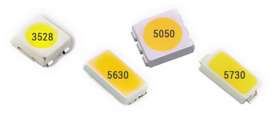
Chip resistors, capacitors, etc.: Size specifications: 0201,0402,0603,0805,1206,1210, 2010, etc.
Tantalum capacitors: size specifications: TANA, TANB, TANC, TANDSOT
Transistor: SOT23, SOT143, SOT89 and other melf cylindrical components: diodes, resistors, etc.
SOIC integrated circuit: size specifications: SOIC08,14,16,18,20,24,28,32
QFP close-pitch integrated circuit PLCC integrated circuit: PLCC20,28,32,44,52,68,84
BGA ball grid array packaged integrated circuits: Array pitch specifications: 1.27,1.00,0.80
CSP integrated circuit: the side length of the component does not exceed 1.2 times the side length of the chip inside, and the microBGA with the array spacing <0.50
There are many evaluation methods for the statistical average diameter of the spray mist particles of the nozzle, usually arithmetic statistical average diameter, geometric statistical average diameter, but the most commonly used is Sauter average, abbreviated as SMD.
The principle is to approximate all the fog particles with spheres of uniform diameter with the same surface area and volume. The diameter of the spheres sought is the Sautel average diameter.
Since this statistical average reflects the physical characteristics of the subject well, it is the most widely used in practice.
Features of SMD
High assembly density, small size and light weight of electronic products. The volume and weight of chip components are only about 1/10 of that of traditional plug-in components. Generally, after SMT is adopted, the volume of electronic products is reduced by 40%~60%, and the weight is reduced by 60%~ 80%.
High reliability and strong anti-vibration ability. The defect rate of solder joints is low.
Good high frequency characteristics. Reduce electromagnetic and radio frequency interference.
It is easy to realize automation and improve production efficiency. Reduce costs by 30%~50%. Save materials, energy, equipment, manpower, time, etc.
SMD inspection
Surface mount component inspection. The main inspection items of components include solderability, pin coplanarity and usability, which should be sampled by the inspection department. To test the solderability of components, stainless steel tweezers can hold the component body and immerse it in a tin pot at 235±5℃ or 230±5℃, and take it out at 2±0.2s or 3±0.5s. Check the soldering end of the solder under a 20 times microscope, and it is required that more than 90% of the soldering end of the component is soldered.
As a processing workshop, the following visual inspections can be done:
⒈Visually or with a magnifying glass, check whether the solder ends or pin surfaces of the components are oxidized or have no contaminants.
⒉The nominal value, specification, model, accuracy, external dimension, etc. of the components should be in accordance with the product process requirements.
⒊The pins of SOT and SOIC cannot be deformed. For multi-lead QFP devices with a lead pitch of less than 0.65mm, the pin coplanarity should be less than 0.1mm (which can be optically detected by the placement machine).
⒋For products that require cleaning, the mark of the components will not fall off after cleaning, and will not affect the performance and reliability of the components (visual inspection after cleaning).
(To Be Continued)


