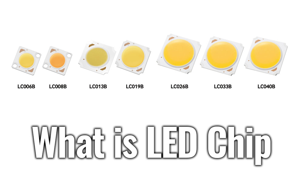
A solid-state semiconductor device. The heart of an LED is a semiconductor wafer. One end of the wafer is attached to a bracket, one end is the negative electrode, and the other end is connected to the positive electrode of the power supply, so that the entire wafer is encapsulated by epoxy resin. Also called LED light emitting chip, it is the core component of LED light, which is also referred to as P-N junction. Its main function is to convert electrical energy into light energy, and the main material of the chip is single crystal silicon. A semiconductor wafer consists of two parts, one is a P-type semiconductor, where holes dominate, and the other end is an N-type semiconductor, where electrons are mainly. But when these two semiconductors are connected, a P-N junction is formed between them. When a current is applied to the wafer through a wire, the electrons are pushed to the P region, where the electrons and holes recombine, and then the energy is emitted in the form of photons. This is the principle of LED light emission. The wavelength of light, which is the color of light, is determined by the material that forms the P-N junction. Fifty years ago, people had learned the basics of the light that semiconductor materials can produce. In 1962, General Electric’s Nick Holonyak Jr. developed the first practical application of visible light-emitting diodes. LED is the abbreviation of light emitting diode (light emitting diode) in English. Its basic structure is a piece of electroluminescent semiconductor material, which is placed on a leaded shelf, and then sealed with epoxy resin around it. In order to protect the role of the internal chip, the shock resistance of the LED is good.
Development history of LED chips
The improvement of chip technology and lower prices are the key to reducing the cost of LED lighting applications. With the improvement of LED chip technology and the improvement of LED luminous efficiency, the cost required for a single LED chip continues to decrease. At the same time, the large-scale production capacity driven by upstream investment and the intensified market competition will also drive down chip prices, which will effectively drive down the cost of LED lighting products. In 2011, the chip quickly changed from oversupply to oversupply, and chip prices fell rapidly. For example, in 2011, the prices of low-power 7.5mil × 7.5mil blue-chip chips and high-power 45mil × 45mil blue-chip chips fell by 55.9% and 55.0%, respectively. Whether it is a high-power LED chip for accent lighting and overall lighting, or a low-power LED chip for decorative lighting and some simple auxiliary lighting, the key to technological upgrade is about how to develop more efficient and stable LED chips. In just a few years, with the help of a series of technological improvements including the new chip structure and the new epitaxial mechanism design of the multiple quantum well structure, the LED’s luminous efficiency has achieved a huge breakthrough. These technological breakthroughs will be the popularization of LED semiconductor lighting Pave the way.
Clips classification
1. MB chip
Definition: MB chip ﹕ Metal Bonding chip ﹔ This chip belongs to UEC’s patented product
Features: 1. The material with high heat dissipation coefficient — Si is used as the substrate, and the heat dissipation is easy.
1. the metal layer to bond (wafer bonding) the epitaxial layer and the substrate, while reflecting photons, to avoid absorption of the substrate.
2.The conductive Si substrate replaces the GaAs substrate and has good thermal conductivity (a thermal conductivity difference of 3 to 4 times), which is more suitable for high driving current fields. 4. The bottom metal reflective layer is conducive to the improvement of light and heat dissipation
3.Size can be increased for high power applications, eg, 42mil MB
2. GB chip
Definition: GB chip ﹕ Glue Bonding chip ﹔ This chip belongs to UEC’s patented product
Features:
1. Transparent sapphire substrate replaces light-absorbing GaAs substrate. Its output power is more than twice that of traditional AS (Absorbable structure) chip. Sapphire substrate is similar to TS chip GaP substrate.
2. The chip emits light on all sides, with excellent pattern
3. LED chip
1. In terms of brightness, the overall brightness has exceeded the level of the TS chip (8.6mil)
2. Dual electrode structure, its high current resistance is slightly worse than TS single electrode TS chip definition and characteristics
4. TS chip
Definition: TS chip ﹕ transparent structure (transparent substrate) chip, this chip belongs to HP’s patented product.
Features:
1. The chip process is complex, much higher than AS LED
2. Excellent reliability
3. Transparent GaP substrate, no light absorption, high brightness
4. Wide application
5. AS chip
Definition: AS chip (Absorbable structure) chip. After nearly 40 years of development efforts, the research and development, production, and sales of this type of chip by the Taiwan LED optoelectronics industry are at a mature stage. Major companies are developing in this area. The level is basically at the same level, and the gap is not large. The mainland chip manufacturing industry started late, and its brightness and reliability still have a certain gap with the Taiwanese industry. The AS chip we are talking about here refers to the UEC AS chip, eg: 712SOL-VR, 709SOL-VR, 712SYM-VR, 709SYM-VR, etc.
Features:
1. Quaternary chip, made by MOVPE process, brighter than conventional chips
2. Excellent reliability
3. Wide application
Structure of LED chip
1. Flip-chip structure
The traditional LED chip uses a front-mounted structure, which is usually coated with a layer of epoxy resin, and sapphire is used as the substrate. On the one hand, due to the poor thermal conductivity of sapphire, the heat generated by the active layer cannot be released in a timely manner, and the sapphire substrate can absorb the light in the active area. Due to the poor thermal conductivity of epoxy resin, heat can only be dissipated by the pins below the chip. Therefore, both front and back aspects cause heat dissipation problems, affecting the performance and reliability of the device. In view of this, LED flip-chip welding technology came into being.
In 2001, LumiLeds developed the AIGalnN power-type flip-chip structure, and the LED chip was flip-chip connected to the silicon substrate. In this way, the heat generated by the high-power LED does not need to pass through the sapphire substrate of the chip, but directly to the silicon or ceramic substrate with higher thermal conductivity, and then to the metal base. Because its active heating area is closer to the heat sink, Reduces internal heat sink thermal resistance. The theoretical calculation of the thermal resistance of this structure can reach a minimum of 1.34K / W, and actually achieve 6-8K / W, and the light output rate has also increased by about 60%. However, the thermal resistance is proportional to the thickness of the heat sink. Because it is limited by the mechanical strength and thermal conductivity of the silicon wafer, it is difficult to further reduce the thermal resistance of the internal heat sink by thinning the silicon wafer, which limits its heat transfer. Further improvement in performance.
2. Vertical structure
LED chips have two basic structures, horizontal and vertical. The so-called lateral structure LED chip means that the two electrodes of the chip are on the same side of the epitaxial wafer. Because the electrodes are on the same side, the lateral flow of current in the n- and p-type confinement layers is not conducive to the diffusion of current and heat dissipation. In contrast, a vertical structure LED chip means that two electrodes are distributed on opposite sides of the epitaxial wafer, and a patterned electrode and all p-type confinement layers are used as the second electrode, so that almost all of the current flows vertically through the LED epitaxial layer, with little lateral flow. Of current. Vertical structure LEDs can be divided into GaP-based LEDs, GaN-based LEDs, and ZnO-based LEDs by material. The LEDs are respectively represented by red and black) and are electrically connected to the positive and negative poles of the heat sink or PCB or circuit board (represented by red and black respectively). The external power supply is connected to the “ten” and “one” poles on the circuit board.
The vertical structure GaN-based LED chip based on sapphire developed by SemiLedS has been on the market since November 2005. There are two basic methods for manufacturing vertical structure LED chips: stripped growth substrate and non-stripped growth substrate. Compared with the horizontal structure LED chip, the vertical structure LED chip has the following obvious advantages:
(l) All manufacturing processes are performed at the wafer level.
(2) High antistatic ability.
(3) No need for gold wires. On the one hand, the package thickness is thin, which can be used to manufacture ultra-thin devices, such as backlights, large screen displays, etc; on the other hand, the yield and reliability are improved.
(4) Perform aging before packaging to reduce production costs.
(5) A larger diameter via / metal filling plug and multiple vias / metal filling plugs can be used to further improve the heat dissipation efficiency of the substrate. This feature is especially important for high-power LEDs. [2]
Important parameters
1. Forward working current If
It refers to the forward current value when the light emitting diode is normally emitting light. In actual use, the IF should be selected below 0.6 · IFm as required.
2. Forward working voltage VF
The working voltage given in the parameter table is obtained at a given forward current. Generally measured at IF = 20mA. The forward working voltage VF of the light-emitting diode is 1.4 to 3V. When the outside temperature rises, VF will drop.
3. V-I characteristics
The relationship between the voltage and current of the light-emitting diode, when the forward voltage is less than a certain value (called a threshold value), the current is extremely small and does not emit light. When the voltage exceeds a certain value, the forward current increases rapidly with the voltage and emits light.
4. Luminous intensity IV
The luminous intensity of a light-emitting diode generally refers to the luminous intensity in the direction of the normal line (the axis of the cylindrical arc tube). If the radiation intensity in this direction is (1/683) W / sr, 1 candela is emitted (symbol cd). Since the intensity of light emitting diodes of general LEDs is small, the unit of candle light (candela, mcd) is often used as the luminous intensity.
LED chip production
For the production of LED chips, the choice of substrate material is the first consideration. Which suitable substrate should be used depends on the requirements of the device and LED device. Three substrate materials: sapphire (Al2O3), silicon (Si), and silicon carbide (SiC).
Advantages of sapphire: 1. Mature production technology and good device quality; 2. Good stability, can be used in high temperature growth process; 3. High mechanical strength, easy to handle and clean.
The shortcomings of sapphire: 1. Lattice mismatch and thermal stress mismatch will cause a large number of defects in the epitaxial layer; 2. Sapphire is an insulator, and two electrodes are made on the upper surface, resulting in a reduction in the effective light emitting area; The lithography and etching processes are increased, and the manufacturing cost is high.
Silicon is a good conductor of heat, so the thermal conductivity of the device can be significantly improved, thereby extending the life of the device.
International Golf Club
The LED chip of silicon carbide substrate (CREE company specially uses SiC material as the substrate), the electrode is an L-shaped electrode, and the current flows vertically. The electrical conductivity and thermal conductivity of devices made with this substrate are very good, which is conducive to making high-power devices with large areas. Advantages: The thermal conductivity of silicon carbide is 490W / m · K, which is more than 10 times higher than that of sapphire substrate. Disadvantages: The manufacturing cost of silicon carbide is high, and the corresponding cost must be reduced to realize its commercialization.
High Power Research
In recent years, the LED upstream industry has developed rapidly. The fierce competition in the market has reduced the cost of chips. However, compared with traditional lighting, the cost is still higher. LEDs must replace traditional lighting. Cost has become an important aspect, and packaging is the decision. An important link in the price of LED light sources. In the future, ultra-low-cost LED lighting will require fewer LED lamp beads and larger chips will be required. Therefore, high-performance high-power LED chips driven by high current have become a must-have field for LED upstream. Institutions and research institutes in the field of semiconductor lighting at home and abroad are committed to the research and exploration of the industrialization of such high-end chips. Although due to the constraints of complex production processes, low product yields, and high costs, there are still many excellent development of high-end products and advanced manufacturing technologies has greatly promoted the industrialization process of power LED chips.
The industry believes that the recognized development route of LED lighting technology is: the luminous efficiency has increased from 25lm / w in 2002 to 75lm / w in 2007, and its luminous efficiency will reach 150lm / w in 2012, and in 2020, when LED chips are commercialized, their Luminous efficiency will exceed 200lm / w; luminous cost will drop from 200 USD / 1000 lumens in 2002 to 20 USD / 1000 lumens in 2007, to 5 USD / 1000 lumens in 2012, and to 2 USD / 1000 by 2020 Lumen; LED lighting began to enter the field of incandescent lighting in 2007, entered the fluorescent lamp market in 2012, and popularly replaced incandescent and fluorescent lamps in 2020.
The average annual growth rate of the global LED market is more than 20%; the high-brightness LED market has grown faster, with an average annual growth rate of 46% from 1995 to 2005, and the market size in 2008 reached $ 5.1 billion, accounting for the proportion of the LED market From 40% in 2001 to more than 80% in 2008, a conservative estimate is that the market size in 2012 is expected to reach $ 11.4 billion. Market demand has driven the development of production links, and large companies in other industries have also moved to this market. Many of the world’s top 500 giant companies have entered the LED blue ocean market. LED semiconductor lighting as a new type of green energy, whether it is the energy saving and economic benefits are very significant, so governments of all countries are vigorously promoting the popularization of LED lighting.
As an emerging industry, LED semiconductor lighting is still in the process of continuous progress. The industry believes that the development path of LED chip luminous efficiency is: from 25lm / w in 2002 to 75lm / w in 2007, the luminous efficiency in 2012 will generally reach 150lm / w, and the luminous efficiency of commercialized LED chips in 2020 will be Exceeded 200lm / w. From 2007, LED lighting began to develop into the field of incandescent lighting, until 2012, it entered the fluorescent lighting market, and will popularly replace today’s incandescent and fluorescent lamps in 2020.
The main problems of LED chips
The main technical difficulties facing LED chips, especially high-power LED chips, are mainly the following:
1. Low luminous efficiency
Although the packaged white LEDs produced by various manufacturers have a light output efficiency of more than 100lm / w, compared to small-sized LED chips, their light output efficiency is still very low. Due to the large size of large-sized LED chips, when light propagates inside the device, the path through which the light passes is longer than that of the small-sized chip, resulting in a greater probability of light absorption by the device material, and a large amount of light is limited to The inside of the device cannot be emitted, resulting in low light efficiency. [1]
2. Uneven current diffusion
For high-power LED chips, large current drive is required (generally 350mA). In order to obtain uniform current diffusion, a reasonable electrode structure needs to be designed so that the current is evenly distributed at the P-type level. Due to the chip size of high-power LED chips Larger, at the same time, it is difficult for the current of the P-type layer to be uniformly diffused at the P-type layer, causing the current to accumulate under the electrode, causing a current crowding effect. Due to the current accumulation effect, that is, the current is mainly concentrated in the area directly below the electrode, the lateral expansion is relatively small, and the current distribution is very uneven, resulting in excessive local current density.
3. Unstable photoelectric characteristics
Under the light-emitting efficiency of high-power LED chip devices, a large amount of light is absorbed inside the device. These absorbed light are converted into thermal energy inside the device, which causes the junction temperature of the LED chip to increase. The increase in junction temperature will not only cause light attenuation. It seriously affects the life of the LED chip. At the same time, the increase in temperature will cause the blue light peak of the chip to shift to the long wavelength direction (that is, red shift). Sexual decline.
4. The luminous efficiency of industrialization research is far lower than the laboratory R & D level
Although the mainstream LED chip manufacturers in the world have reached a high level of research and development in the laboratory, the level of industrialization research is still below. The main reason for this is that industrialization must not only consider the cost requirements but also take into account the production process Complexity and chip yield issues.
Common problems in using technology
Analysis of the problems often encountered in the use of LED chips: The forward pressure drop can also be formed in other packaging processes. The main reasons are insufficient silver glue curing, and the touch resistance of the bracket or chip electrode is large or the touch resistance is unstable.
1. Forward voltage drop
A: One is that the electrode and the light-emitting material are ohmic touch, but the touch resistance is large, mainly formed by the low concentration of the data substrate or the electrode is incomplete.
B: One is the non-ohmic touch between the electrode and the material, which mainly occurs in the squeezing or pinching when the first layer of electrode is transpired during the preparation of the chip electrode, and the orientation is scattered.
Clips For a chip with a forward voltage drop, when the fixed voltage test is performed, the current passing through the chip is small, and then the dark spot is reflected. There is also a kind of dark light that the chip’s own light emitting power is low and the forward voltage drop is normal.
2. Difficult welding – Firstly, there is no sticking, the electrode is dropped, and the electrode is penetrated
A: Not sticky: mainly because of electrode surface oxidation or glue
B: There are weak touches with the luminous materials and the thick wire bonding layer is not strong. In the meantime, the thick layer drops.
C: Breakthrough electrode: usually related to the chip data, the data is brittle and the strength is not easy to penetrate the electrode, usually GAALAS data (such as high red, infrared chip) is easier to penetrate the electrode than GAP data,
D: Pressure welding debugging should be adjusted from welding temperature, ultrasonic power, ultrasonic moment, pressure, gold ball size, bracket positioning, etc.
3. Difference in luminous color
A: There is a significant difference in the luminous color of the same chip. The main reason is that the epitaxial wafer data is questionable. The quantum layout of the ALGAINP four-element data is very thin. It is difficult to ensure that the components of each region are common. (The component determines the forbidden band width, and the forbidden band determines the wavelength).
B: GAP yellow-green chip, the emission wavelength will not have a large error, but because the human eye is sensitive to the color of this band, it is easy to detect yellowish and greenish. Because the wavelength is determined by epitaxial wafer data, the smaller the area, the smaller the concept of rendering color error, so there is a nearby selection method in M / T operations.
C: The light emitting color of GAP red chip is orange-yellow. This is because the light emitting mechanism is a direct leap forward. Affected by the concentration of impurities, when the current density increases, impurity level shifts and full luminescence are prone to occur, and the luminescence begins to turn orange-yellow.
4. Gate fluid effect
A: The light-emitting diode cannot be turned on under normal voltage. When the voltage is increased to a certain level, the current changes suddenly.
B: The reason for the appearance of the sluice fluid is that the epitaxial wafer grows in the opposite direction when the epitaxial wafer grows. The LED with this appearance has a hidden forward voltage drop measured at IF = 20MA. The application process is due to the North and South voltage Large, it is not bright, you can use the test information instrument to test the curve from the transistor diagram, you can also find through the small current IF = 10UA forward voltage drop, the small forward voltage drop is significantly larger, then Can be the result of this question.
5. Reverse leakage
A: Reason: epitaxial data, chip manufacturing, equipment packaging. The test usually has a reverse leakage current of 10UA at 5V, and it can also test the reverse voltage at a fixed reverse current.
B: The reverse characteristics of different types of LEDs are quite different: ordinary green, ordinary yellow chip reverse breakdown can reach more than one hundred volts, and ordinary chips are between ten and twenty volts.
C: The reverse leakage caused by epitaxy is mainly caused by the internal layout defects of the PN junction. During the chip manufacturing process, the side surface is not corroded or silver glue wire is attached to the test surface. It is strictly prohibited to use organic solutions to distribute silver glue. To avoid the silver glue crawling through the capillary appearance to the knot area.
 A solid-state semiconductor device. The heart of an LED is a semiconductor wafer. One end of the wafer is attached to a bracket, one end is the negative electrode, and the other end is connected to the positive electrode of the power supply, so that the entire wafer is encapsulated by epoxy resin. Also called LED light emitting chip, it is the core component of LED light, which is also referred to as P-N junction. Its main function is to convert electrical energy into light energy, and the main material of the chip is single crystal silicon. A semiconductor wafer consists of two parts, one is a P-type semiconductor, where holes dominate, and the other end is an N-type semiconductor, where electrons are mainly. But when these two semiconductors are connected, a P-N junction is formed between them. When a current is applied to the wafer through a wire, the electrons are pushed to the P region, where the electrons and holes recombine, and then the energy is emitted in the form of photons. This is the principle of LED light emission. The wavelength of light, which is the color of light, is determined by the material that forms the P-N junction. Fifty years ago, people had learned the basics of the light that semiconductor materials can produce. In 1962, General Electric’s Nick Holonyak Jr. developed the first practical application of visible light-emitting diodes. LED is the abbreviation of light emitting diode (light emitting diode) in English. Its basic structure is a piece of electroluminescent semiconductor material, which is placed on a leaded shelf, and then sealed with epoxy resin around it. In order to protect the role of the internal chip, the shock resistance of the LED is good.
 The improvement of chip technology and lower prices are the key to reducing the cost of LED lighting applications. With the improvement of LED chip technology and the improvement of LED luminous efficiency, the cost required for a single LED chip continues to decrease. At the same time, the large-scale production capacity driven by upstream investment and the intensified market competition will also drive down chip prices, which will effectively drive down the cost of LED lighting products. In 2011, the chip quickly changed from oversupply to oversupply, and chip prices fell rapidly. For example, in 2011, the prices of low-power 7.5mil × 7.5mil blue-chip chips and high-power 45mil × 45mil blue-chip chips fell by 55.9% and 55.0%, respectively. Whether it is a high-power LED chip for accent lighting and overall lighting, or a low-power LED chip for decorative lighting and some simple auxiliary lighting, the key to technological upgrade is about how to develop more efficient and stable LED chips. In just a few years, with the help of a series of technological improvements including the new chip structure and the new epitaxial mechanism design of the multiple quantum well structure, the LED’s luminous efficiency has achieved a huge breakthrough. These technological breakthroughs will be the popularization of LED semiconductor lighting Pave the way.
 LED chips have two basic structures, horizontal and vertical. The so-called lateral structure LED chip means that the two electrodes of the chip are on the same side of the epitaxial wafer. Because the electrodes are on the same side, the lateral flow of current in the n- and p-type confinement layers is not conducive to the diffusion of current and heat dissipation. In contrast, a vertical structure LED chip means that two electrodes are distributed on opposite sides of the epitaxial wafer, and a patterned electrode and all p-type confinement layers are used as the second electrode, so that almost all of the current flows vertically through the LED epitaxial layer, with little lateral flow. Of current. Vertical structure LEDs can be divided into GaP-based LEDs, GaN-based LEDs, and ZnO-based LEDs by material. The LEDs are respectively represented by red and black) and are electrically connected to the positive and negative poles of the heat sink or PCB or circuit board (represented by red and black respectively). The external power supply is connected to the “ten” and “one” poles on the circuit board.
 In recent years, the LED upstream industry has developed rapidly. The fierce competition in the market has reduced the cost of chips. However, compared with traditional lighting, the cost is still higher. LEDs must replace traditional lighting. Cost has become an important aspect, and packaging is the decision. An important link in the price of LED light sources. In the future, ultra-low-cost LED lighting will require fewer LED lamp beads and larger chips will be required. Therefore, high-performance high-power LED chips driven by high current have become a must-have field for LED upstream. Institutions and research institutes in the field of semiconductor lighting at home and abroad are committed to the research and exploration of the industrialization of such high-end chips. Although due to the constraints of complex production processes, low product yields, and high costs, there are still many excellent development of high-end products and advanced manufacturing technologies has greatly promoted the industrialization process of power LED chips.
 The industry believes that the recognized development route of LED lighting technology is: the luminous efficiency has increased from 25lm / w in 2002 to 75lm / w in 2007, and its luminous efficiency will reach 150lm / w in 2012, and in 2020, when LED chips are commercialized, their Luminous efficiency will exceed 200lm / w; luminous cost will drop from 200 USD / 1000 lumens in 2002 to 20 USD / 1000 lumens in 2007, to 5 USD / 1000 lumens in 2012, and to 2 USD / 1000 by 2020 Lumen; LED lighting began to enter the field of incandescent lighting in 2007, entered the fluorescent lamp market in 2012, and popularly replaced incandescent and fluorescent lamps in 2020.
 As an emerging industry, LED semiconductor lighting is still in the process of continuous progress. The industry believes that the development path of LED chip luminous efficiency is: from 25lm / w in 2002 to 75lm / w in 2007, the luminous efficiency in 2012 will generally reach 150lm / w, and the luminous efficiency of commercialized LED chips in 2020 will be Exceeded 200lm / w. From 2007, LED lighting began to develop into the field of incandescent lighting, until 2012, it entered the fluorescent lighting market, and will popularly replace today’s incandescent and fluorescent lamps in 2020.