When you see that the LED light on the board produces a color that changes over time, do you know how it is achieved?
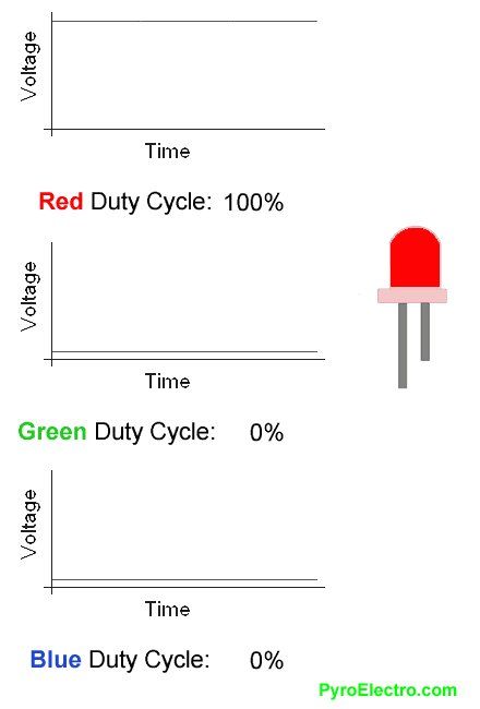
Partners who have done MCU program or FPGA logic programming should know (there are many articles about PWM also specifically introduced), it is obtained by adjusting the brightness of the three colors of R, G, and B in the following way. Yes, the individual changes of the lights of each color (luminous frequency) are combined together in the distance, and what you see is the color change of a light.
The brightness of each color of R, G, B is controlled by PWM to synthesize various colors.
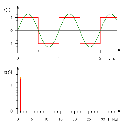
Also on the oscilloscope, when you see the waveform on the left in the figure below (the thick solid line) in the time domain, do you know how it is formed? In fact, it is obtained by synthesizing two waveforms of different frequencies (after FFT analysis).
Are you enlightened so far?
When we “use one eye” to see things from a fixed angle, the amount of information we can obtain is limited. Sometimes it is difficult to intuitively judge its essence, but if we turn one angle, we increase a dimension (open the other one). (Eye) to see the same things, you can see more laws and origins.
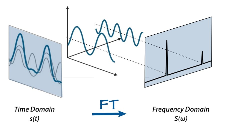
If the oscilloscope is an eye of our engineers, we actually have another eye to open. For example, spectrum analyzers and logic analyzers, etc. These tools can help us to observe more information that is difficult to intuitively draw conclusions at a fixed point or a plane from different angles and different dimensions, so make good use of these tools Can help us locate the problem faster. Especially the frequency domain information corresponding to the time domain used in our common sense.
The following animated picture visually demonstrates that the class components of a square wave signal are very complicated. Through FFT transformation, we can decompose the time-domain waveform (varying with time) in the above picture into countless waveforms of different frequency components.
When expanded, it looks like the following:
When debugging analog signals, RF signals, and even power and grounding, the frequency spectrum of the signal is as important as the waveform in the time domain. Therefore, watching the frequency spectrum is an essential skill for our electronic engineers. If not, it means you He is a crappy engineer.
Many engineers have never touched a spectrum analyzer, which is why they think the spectrum analyzer is very mysterious.
If you can see with one eye, you think one eye is enough. It doesn’t matter whether you have the other eye or not, so even if you have another eye, you don’t bother to learn to open it.
Spectrum analyzers used to be very expensive. I remember that around 1997 we had to rent a spectrum analyzer in the laboratory when debugging the RF signal. It is said that the HP spectrum analyzer used at that time sold for more than a Mercedes-Benz luxury car. The Mercedes-Benz at that time was $200,000 in the minds of many people. . If it weren’t necessary for the project, no one would pay for such expensive equipment.
At first glance, every component of the spectrum analyzer needs to be polished by an old engineer with many years of experience. However, the cost of the components is not worth a Mercedes-Benz. It was so expensive at that time, mainly because of the scarcity of goods and too few people, so it was extremely expensive. If its market volume is as large as today’s smart phones, it is estimated that the price of this thing will be hit within a few hundred dollars, because the circuit inside is really not as complicated as a smart phone.
Some friends said that we don’t have a spectrum analyzer here. What should I do? In fact, there is a workaround – almost all digital oscilloscopes now have an FFT function, which can be used. Although it is not as accurate as a real spectrum analyzer, it can at least help you get a lot of information from the frequency domain. Why do current digital oscilloscopes have FFT function? Because this function in the “digital domain” does not increase any system cost. Engineers who know how to play FPGA know that the so-called FFT is to use more logic resources in the FPGA without increasing the cost of any device.
We are used to some concepts in the time domain, and we need to adapt to another space. It is necessary to deeply understand some basic concepts in the frequency domain, and analyze the meaning of each indicator from the perspective of signal composition, and the relationship between the numbers in the frequency domain and the time domain.
Just like you have learned plane geometry, one day you have to learn solid geometry, you will find that there are many concepts that cannot be imagined by plane geometry alone. But once you are familiar with these new concepts, the sense of space in your mind will be as clear and free as three-dimensional geometry.
Reasons for dimming high-brightness LEDs
The main reason for failure
As a kind of electrical equipment, LED also has many possible errors. However, in practice, LEDs are of solid quality and strong performance, and the “failure” is likely to be the result of light. When the light output is lower than 70% of the theoretical design value, it is due to the micro thread dislocation introduced in the wafer manufacturing process.
The defects in the LED chip material will grow rapidly at higher temperatures and reappear one by one until it invades the light-emitting area and forms a large number of non-radiative recombination centers, which seriously reduces the luminous efficiency of the LED. In addition, under high temperature conditions, micro-defects in the material and fast-expanding impurities from the interface and the circuit board will also be introduced into the light-emitting area, forming a large number of deep layers, which will also accelerate the light attenuation of the LED device. Transparent epoxy resin will denature at high temperature. ——Yellowing will affect its light transmission performance. The higher the operating temperature, the faster the process will proceed. This is another main reason for the attenuation of LED lights. The light attenuation of the phosphor covered on the LED chip is also the main reason for the light attenuation of the LED, because the attenuation of the phosphor at high temperature is very serious.
The increase in temperature will reduce the luminous efficiency of the LED lamp, the reasons include the following:
When the temperature increases, the concentration of electrons and holes increases, the band gap decreases, the electron mobility decreases, and the number of photons decreases.
When the temperature rises, the possibility of electrons and holes in the potential well is reduced, resulting in non-radiative recombination (heating), thereby reducing the internal quantum efficiency of the LED.
The increase in temperature causes the blue peak of the chip to move to the long wave direction, which causes the emission wavelength of the chip and the excitation wavelength of the phosphor to be mismatched, which also leads to a decrease in the extraction efficiency of external light.
In a white LED light source, as the temperature increases, the quantum efficiency of the phosphor decreases, the light emission decreases, and the external light extraction efficiency of the LED substrate decreases.
The properties of silica gel are greatly affected by the ambient temperature. As the temperature rises, the thermal stress inside the silica gel increases, causing the refractive index of the silica gel to decrease, thereby affecting the light efficiency of the LED lamp.
High-quality high-efficiency LEDs often have a lifespan of more than 5 years without rapid decline. As time goes by, the brightness of the LED will gradually decrease. A well-designed LED lighting system can continue to use the light source for 60,000 or even 80,000 hours before the lighting is no longer sufficient to complete the expected work.
Why does the chip brightness become low? What measures can be taken to stop this recession? We will work with you to understand the physics behind the photon generation of LEDs to explore what will happen to the new facility and why the chip will age, resulting in an inevitable decline in performance.
Design engineers can take many measures to maximize the service life of LEDs, and major LED suppliers (such as Seoul Semiconductor, Cree, OSRAM and Bridgelux) have made great efforts to improve the next generation of commercial LED chips.
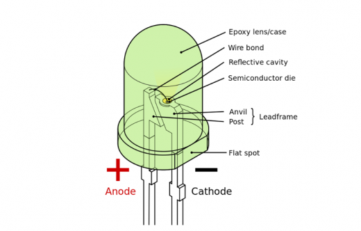
Basic characteristics
When a forward bias is applied to both ends of the PN junction, due to the lowering of the PN junction barrier, the positive charge in the P region will diffuse to the N region, and the electrons in the N region will also diffuse to the P region, forming an imbalance in the two regions at the same time The accumulation of electric charge. For a real PN junction device, the carrier concentration in the P region is usually much greater than that in the N region, causing the accumulation of unbalanced holes in the N region to be much greater than the accumulation of electrons in the P region (for NP junctions, the situation is just the opposite).
Since the minority carriers produced by current injection are unstable, for the PN junction system, the unbalanced holes injected into the valence band must recombine with the electrons in the conduction band, and the excess energy will be transferred in the form of light. External radiation, this is the basic principle of LED luminescence.
That is just an explanation acceptable to the general public. But the actual situation is more complicated. Why does the light output of the LED decrease over time? To understand this, it is necessary for us to have a deeper understanding of optics.
Generally, the larger the band gap, the larger the radiated energy address, and the corresponding photon has a shorter wavelength; conversely, the smaller the band gap, the smaller the energy radiated, and the corresponding photon has a longer wavelength. For semiconductor materials such as GaAsP, GaInAIP, InGaN, GaAIAs, the emission wavelength corresponding to the band gap is just in the visible light region of 380-780nm, thus laying a broad space for the development and application of LEDs.
The basic structure of LED devices can generally be classified into two categories, one is for traditional LEDs such as Gap, GaAsP, AIGaA, etc., which usually adopt liquid phase epitaxy or gas phase epitaxy-r. Art in GaP or GaA.
A simple structure of PN junction or NP junction type is grown on the substrate. In order to improve the luminous intensity, there are also heterostructures. The substrate of this type of device is often part of the PN junction, or P-type region, or N-type region. Therefore, the quality of the substrate of this type of device will directly affect the electrical and optoelectronic properties of the device. A substrate with a proper doping concentration is essential to improve the quality of the epitaxial layer and reduce the series resistance.
The absorption of the emitted light by the substrate is also an important issue. General GaAsP devices use GaAs substrates, and the use of GaP substrates can significantly improve the luminous efficiency. This is because after replacing GaA with transparent GaP, the LED chip changes from surface emission to three-dimensional emission, which greatly reduces the absorption of light by the substrate. In addition, the epitaxial layer should maintain a high carrier concentration to ensure a sufficiently high efficiency.
The second type of structure is mainly for ultra-bright InGaAIP red-yellow light and InGaN blue-green light devices. The basic structure of this type of device usually includes four areas: the substrate area, the Bragg reflection area, the DH or MQW light-emitting area, and the window area.
Such devices are generally prepared by MOCVD epitaxial process. A good substrate is also the basis of the entire epitaxial process. For InGaA1P materials, GaAs materials are usually used as substrates. When the total atomic content of In is 0.25, the lattice of InGaAIP material The constant will be well matched with GaAs, and a high-quality epitaxial layer can be obtained. For GaN-based devices, due to the difficulty of obtaining GaN bulk crystal materials, sapphire or sic is generally used as an epitaxial substrate.
The basic structure of LED
Bragg reflection area–For InGaA1P devices, since GaA as the substrate absorbs red and yellow light strongly, a Bragg reflection area is usually grown between the substrate and the light-emitting area to effectively reflect the light radiation from the light-emitting area. Thereby improving the light-emitting performance of the device. For GaN-based LED devices, since sapphire or sic materials do not have strong absorption of light, it is generally not necessary to add the Bragg reflection zone.
Light-emitting area-This area is the core of the entire device. The use of double heterojunction or quantum well structure can greatly improve the electro-optical conversion efficiency. The last layer is the window area. Generally, the material in this area has a large forbidden band width and can effectively transmit the light radiation from the light-emitting area. Secondly, the material of the window area should have a higher carrier concentration and a low resistivity in order to achieve better current expansion and allow the operating current to flow evenly through the entire PN junction area. In order to further improve the luminous efficiency and power dissipation, many new-type LED devices are under development, the most typical ones are GaP transparent substrate, metal film reflection, truncated inverted cone, surface texture and other structures.